

2Gb: x4, x8, x16 DDR3 SDRAM - Micron
2Gb: x4, x8, x16 DDR3 SDRAM - Micron
2Gb: x4, x8, x16 DDR3 SDRAM - Micron

You also want an ePaper? Increase the reach of your titles
YUMPU automatically turns print PDFs into web optimized ePapers that Google loves.
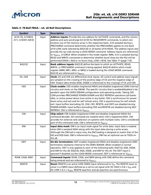
Table 3: 78-Ball FBGA – <strong>x4</strong>, <strong>x8</strong> Ball Descriptions<br />
Symbol Type Description<br />
A[14:13], A12/BC#,<br />
A11, A10/AP, A[9:0]<br />
<strong>2Gb</strong>: <strong>x4</strong>, <strong>x8</strong>, <strong>x16</strong> <strong>DDR3</strong> <strong>SDRAM</strong><br />
Ball Assignments and Descriptions<br />
Input Address inputs: Provide the row address for ACTIVATE commands, and the column<br />
address and auto precharge bit (A10) for READ/WRITE commands, to select one<br />
location out of the memory array in the respective bank. A10 sampled during a<br />
PRECHARGE command determines whether the PRECHARGE applies to one bank<br />
(A10 LOW, bank selected by BA[2:0]) or all banks (A10 HIGH). The address inputs also<br />
provide the op-code during a LOAD MODE command. Address inputs are referenced<br />
to V REFCA. A12/BC#: When enabled in the mode register (MR), A12 is sampled during<br />
READ and WRITE commands to determine whether burst chop (on-the-fly) will be<br />
performed (HIGH = BL8 or no burst chop, LOW = BC4). See Table 71 (page 114).<br />
BA[2:0] Input Bank address inputs: BA[2:0] define the bank to which an ACTIVATE, READ,<br />
WRITE, or PRECHARGE command is being applied. BA[2:0] define which mode<br />
register (MR0, MR1, MR2, or MR3) is loaded during the LOAD MODE command.<br />
BA[2:0] are referenced to VREFCA. CK, CK# Input Clock: CK and CK# are differential clock inputs. All control and address input signals<br />
are sampled on the crossing of the positive edge of CK and the negative edge of<br />
CK#. Output data strobe (DQS, DQS#) is referenced to the crossings of CK and CK#.<br />
CKE Input Clock enable: CKE enables (registered HIGH) and disables (registered LOW) internal<br />
circuitry and clocks on the DRAM. The specific circuitry that is enabled/disabled is dependent<br />
upon the <strong>DDR3</strong> <strong>SDRAM</strong> configuration and operating mode. Taking CKE<br />
LOW provides PRECHARGE POWER-DOWN and SELF REFRESH operations (all banks<br />
idle), or active power-down (row active in any bank). CKE is synchronous for powerdown<br />
entry and exit and for self refresh entry. CKE is asynchronous for self refresh<br />
exit. Input buffers (excluding CK, CK#, CKE, RESET#, and ODT) are disabled during<br />
POWER-DOWN. Input buffers (excluding CKE and RESET#) are disabled during SELF<br />
REFRESH. CKE is referenced to VREFCA. CS# Input Chip select: CS# enables (registered LOW) and disables (registered HIGH) the<br />
command decoder. All commands are masked when CS# is registered HIGH. CS#<br />
provides for external rank selection on systems with multiple ranks. CS# is considered<br />
part of the command code. CS# is referenced to VREFCA. DM Input Input data mask: DM is an input mask signal for write data. Input data is masked<br />
when DM is sampled HIGH along with the input data during a write access.<br />
Although the DM ball is input-only, the DM loading is designed to match that of the<br />
DQ and DQS balls. DM is referenced to VREFDQ. DM has an optional use as TDQS on<br />
the <strong>x8</strong>.<br />
ODT Input On-die termination: ODT enables (registered HIGH) and disables (registered LOW)<br />
termination resistance internal to the <strong>DDR3</strong> <strong>SDRAM</strong>. When enabled in normal<br />
operation, ODT is only applied to each of the following balls: DQ[7:0], DQS, DQS#,<br />
and DM for the <strong>x8</strong>; DQ[3:0], DQS, DQS#, and DM for the <strong>x4</strong>. The ODT input is<br />
ignored if disabled via the LOAD MODE command. ODT is referenced to VREFCA. RAS#, CAS#, WE# Input Command inputs: RAS#, CAS#, and WE# (along with CS#) define the command<br />
being entered and are referenced to VREFCA. RESET# Input Reset: RESET# is an active LOW CMOS input referenced to VSS. The RESET# input receiver<br />
is a CMOS input defined as a rail-to-rail signal with DC HIGH � 0.8 × VDD and<br />
DC LOW � 0.2 × VDDQ. RESET# assertion and de-assertion are asynchronous.<br />
PDF: 09005aef826aaadc<br />
<strong>2Gb</strong>_<strong>DDR3</strong>_<strong>SDRAM</strong>.pdf – Rev. P 2/12 EN 18 <strong>Micron</strong> Technology, Inc. reserves the right to change products or specifications without notice.<br />
� 2006 <strong>Micron</strong> Technology, Inc. All rights reserved.


