

2Gb: x4, x8, x16 DDR3 SDRAM - Micron
2Gb: x4, x8, x16 DDR3 SDRAM - Micron
2Gb: x4, x8, x16 DDR3 SDRAM - Micron

Create successful ePaper yourself
Turn your PDF publications into a flip-book with our unique Google optimized e-Paper software.
<strong>2Gb</strong>: <strong>x4</strong>, <strong>x8</strong>, <strong>x16</strong> <strong>DDR3</strong> <strong>SDRAM</strong><br />
Command and Address Setup, Hold, and Derating<br />
Command and Address Setup, Hold, and Derating<br />
The total tIS (setup time) and tIH (hold time) required is calculated by adding the data<br />
sheet tIS (base) and tIH (base) values (see Table 59; values come from Table 57<br />
(page 77)) to the �tIS and �tIH derating values (see Table 60 (page 98) and Table 61<br />
(page 98)), respectively. Example: tIS (total setup time) = tIS (base) + �tIS. For a valid<br />
transition, the input signal has to remain above/below VIH(AC)/VIL(AC) for some time<br />
tVAC (see Table 61 (page 98)).<br />
Although the total setup time for slow slew rates might be negative (for example, a valid<br />
input signal will not have reached VIH(AC)/VIL(AC) at the time of the rising clock transition),<br />
a valid input signal is still required to complete the transition and to reach<br />
VIH(AC)/VIL(AC) (see Figure 13 (page 47) for input signal requirements). For slew rates that<br />
fall between the values listed in Table 61 (page 98) and Table 64 (page 100), the derating<br />
values may be obtained by linear interpolation.<br />
Setup ( tIS) nominal slew rate for a rising signal is defined as the slew rate between the<br />
last crossing of VREF(DC) and the first crossing of VIH(AC)min. Setup ( tIS) nominal slew rate<br />
for a falling signal is defined as the slew rate between the last crossing of VREF(DC) and<br />
the first crossing of VIL(AC)max. If the actual signal is always earlier than the nominal slew<br />
rate line between the shaded VREF(DC)-to-AC region, use the nominal slew rate for derating<br />
value (see Figure 32 (page 101)). If the actual signal is later than the nominal slew<br />
rate line anywhere between the shaded VREF(DC)-to-AC region, the slew rate of a tangent<br />
line to the actual signal from the AC level to the DC level is used for derating value (see<br />
Figure 34 (page 103)).<br />
Hold ( tIH) nominal slew rate for a rising signal is defined as the slew rate between the<br />
last crossing of VIL(DC)max and the first crossing of VREF(DC). Hold ( tIH) nominal slew rate<br />
for a falling signal is defined as the slew rate between the last crossing of VIH(DC)min and<br />
the first crossing of VREF(DC). If the actual signal is always later than the nominal slew<br />
rate line between the shaded DC-to-VREF(DC) region, use the nominal slew rate for derating<br />
value (see Figure 33 (page 102)). If the actual signal is earlier than the nominal slew<br />
rate line anywhere between the shaded DC-to-VREF(DC) region, the slew rate of a tangent<br />
line to the actual signal from the DC level to the VREF(DC) level is used for derating value<br />
(see Figure 35 (page 104)).<br />
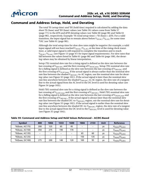
Table 59: Command and Address Setup and Hold Values Referenced – AC/DC-Based<br />
Symbol 800 1066 1333 1600 1866 2133 Unit Reference<br />
tIS(base, AC175) 200 125 65 45 – – ps VIH(AC)/VIL(AC) t IS(base, AC150) 350 275 190 170 – – ps VIH(AC)/V IL(AC)<br />
t IS(base, AC135) – – – – 65 60 ps VIH(AC)/V IL(AC)<br />
t IS(base, AC125) – – – – 150 135 ps VIH(AC)/V IL(AC)<br />
t IH(base, DC100) 275 200 140 120 100 95 ps VIH(DC)/V IL(DC)<br />
PDF: 09005aef826aaadc<br />
<strong>2Gb</strong>_<strong>DDR3</strong>_<strong>SDRAM</strong>.pdf – Rev. P 2/12 EN 97 <strong>Micron</strong> Technology, Inc. reserves the right to change products or specifications without notice.<br />
� 2006 <strong>Micron</strong> Technology, Inc. All rights reserved.


