

2Gb: x4, x8, x16 DDR3 SDRAM - Micron
2Gb: x4, x8, x16 DDR3 SDRAM - Micron
2Gb: x4, x8, x16 DDR3 SDRAM - Micron

Create successful ePaper yourself
Turn your PDF publications into a flip-book with our unique Google optimized e-Paper software.
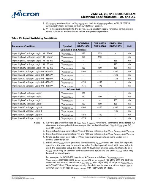
Table 25: Input Switching Conditions<br />
<strong>2Gb</strong>: <strong>x4</strong>, <strong>x8</strong>, <strong>x16</strong> <strong>DDR3</strong> <strong>SDRAM</strong><br />
Electrical Specifications – DC and AC<br />
4. V REFDQ(DC) may transition to V REFDQ(SR) and back to V REFDQ(DC) when in SELF REFRESH,<br />
within restrictions outlined in the SELF REFRESH section.<br />
5. V TT is not applied directly to the device. V TT is a system supply for signal termination resistors.<br />
Minimum and maximum values are system-dependent.<br />
<strong>DDR3</strong>-800 <strong>DDR3</strong>-1333 <strong>DDR3</strong>-1866<br />
Parameter/Condition Symbol <strong>DDR3</strong>-1066 <strong>DDR3</strong>-1600 <strong>DDR3</strong>-2133 Unit<br />
Command and Address<br />
Input high AC voltage: Logic 1 @ 175mV VIH(AC175)min 175 175 – mV<br />
Input high AC voltage: Logic 1 @ 150mV VIH(AC150)min 150 150 – mV<br />
Input high AC voltage: Logic 1 @ 135 mV VIH(AC135)min – – 135 mV<br />
Input high AC voltage: Logic 1 @ 125 mV VIH(AC125)min – – 125 mV<br />
Input high DC voltage: Logic 1 @ 100 mV VIH(DC100)min 100 100 100 mV<br />
Input low DC voltage: Logic 0 @ –100mV VIL(DC100)max –100 –100 –100 mV<br />
Input low AC voltage: Logic 0 @ –125mV VIL(AC125)max – – –125 mV<br />
Input low AC voltage: Logic 0 @ –135mV VIL(AC135)max – – –135 mV<br />
Input low AC voltage: Logic 0 @ –150mV VIL(AC150)max –150 –150 – mV<br />
Input low AC voltage: Logic 0 @ –175mV VIL(AC175)max DQ and DM<br />
–175 –175 – mV<br />
Input high AC voltage: Logic 1 VIH(AC175)min 175 – – mV<br />
Input high AC voltage: Logic 1 VIH(AC150)min 150 150 – mV<br />
Input high AC voltage: Logic 1 VIH(AC135)min – – 135 mV<br />
Input high DC voltage: Logic 1 VIH(DC100)min 100 100 100 mV<br />
Input low DC voltage: Logic 0 VIL(DC100)max –100 –100 –100 mV<br />
Input low AC voltage: Logic 0 VIL(AC135)max – – –135 mV<br />
Input low AC voltage: Logic 0 VIL(AC150)max –150 –150 – mV<br />
Input low AC voltage: Logic 0 VIL(AC175)max –175 – – mV<br />
Notes: 1. All voltages are referenced to V REF. V REF is V REFCA for control, command, and address. All<br />
slew rates and setup/hold times are specified at the DRAM ball. V REF is V REFDQ for DQ<br />
and DM inputs.<br />
2. Input setup timing parameters ( t IS and t DS) are referenced at V IL(AC)/V IH(AC), not V REF(DC).<br />
3. Input hold timing parameters ( t IH and t DH) are referenced at V IL(DC)/V IH(DC), not V REF(DC).<br />
4. Single-ended input slew rate = 1 V/ns; maximum input voltage swing under test is<br />
900mV (peak-to-peak).<br />
5. When two V IH(AC) values (and two corresponding V IL(AC) values) are listed for a specific<br />
speed bin, the user may choose either value for the input AC level. Whichever value is<br />
used, the associated setup time for that AC level must also be used. Additionally, one<br />
V IH(AC) value may be used for address/command inputs and the other V IH(AC) value may<br />
be used for data inputs.<br />
For example, for <strong>DDR3</strong>-800, two input AC levels are defined: V IH(AC175),min and<br />
V IH(AC150),min (corresponding V IL(AC175),min and V IL(AC150),min). For <strong>DDR3</strong>-800, the address/<br />
command inputs must use either V IH(AC175),min with t IS(AC175) of 200ps or V IH(AC150),min<br />
with t IS(AC150) of 350ps; independently, the data inputs must use either V IH(AC175),min<br />
with t DS(AC175) of 75ps or V IH(AC150),min with t DS(AC150) of 125ps.<br />
PDF: 09005aef826aaadc<br />
<strong>2Gb</strong>_<strong>DDR3</strong>_<strong>SDRAM</strong>.pdf – Rev. P 2/12 EN 46 <strong>Micron</strong> Technology, Inc. reserves the right to change products or specifications without notice.<br />
� 2006 <strong>Micron</strong> Technology, Inc. All rights reserved.


