- Page 1 and 2:
DDR3 SDRAM MT41J512M4 - 64 Meg x 4
- Page 3 and 4:
2Gb: x4, x8, x16 DDR3 SDRAM Feature
- Page 5 and 6:
2Gb: x4, x8, x16 DDR3 SDRAM Feature
- Page 7 and 8:
2Gb: x4, x8, x16 DDR3 SDRAM Feature
- Page 9 and 10:
2Gb: x4, x8, x16 DDR3 SDRAM Feature
- Page 11 and 12:
State Diagram Figure 2: Simplified
- Page 13 and 14:
2Gb: x4, x8, x16 DDR3 SDRAM Functio
- Page 15 and 16:
Figure 4: 256 Meg x 8 Functional Bl
- Page 17 and 18: Figure 7: 96-Ball FBGA - x16 (Top V
- Page 19 and 20: Table 3: 78-Ball FBGA - x4, x8 Ball
- Page 21 and 22: Table 4: 96-Ball FBGA - x16 Ball De
- Page 23 and 24: Figure 9: 78-Ball FBGA - x4, x8 (HX
- Page 25 and 26: Figure 11: 96-Ball FBGA - x16 (JT)
- Page 27 and 28: Input/Output Capacitance Table 6: D
- Page 29 and 30: Figure 12: Thermal Measurement Poin
- Page 31 and 32: Table 9: I DD0 Measurement Loop CK,
- Page 33 and 34: 2Gb: x4, x8, x16 DDR3 SDRAM Electri
- Page 35 and 36: Table 14: I DD4R Measurement Loop C
- Page 37 and 38: Table 16: I DD5B Measurement Loop C
- Page 39 and 40: Table 18: I DD7 Measurement Loop CK
- Page 41 and 42: Electrical Characteristics - I DD S
- Page 43 and 44: Table 21: I DD Maximum Limits - Die
- Page 45 and 46: Electrical Specifications - DC and
- Page 47 and 48: Figure 13: Input Signal 0.925V 0.85
- Page 49 and 50: Table 28: Differential Input Operat
- Page 51 and 52: Figure 18: Definition of Differenti
- Page 53 and 54: Figure 19: Nominal Slew Rate Defini
- Page 55 and 56: ODT Characteristics Figure 21: ODT
- Page 57 and 58: Table 33: R TT Effective Impedances
- Page 59 and 60: Figure 23: t AON and t AOF Definiti
- Page 61 and 62: Output Driver Impedance Figure 26:
- Page 63 and 64: 34 Ohm Driver The 34� driver’s
- Page 65 and 66: Alternative 40 Ohm Driver Table 45:
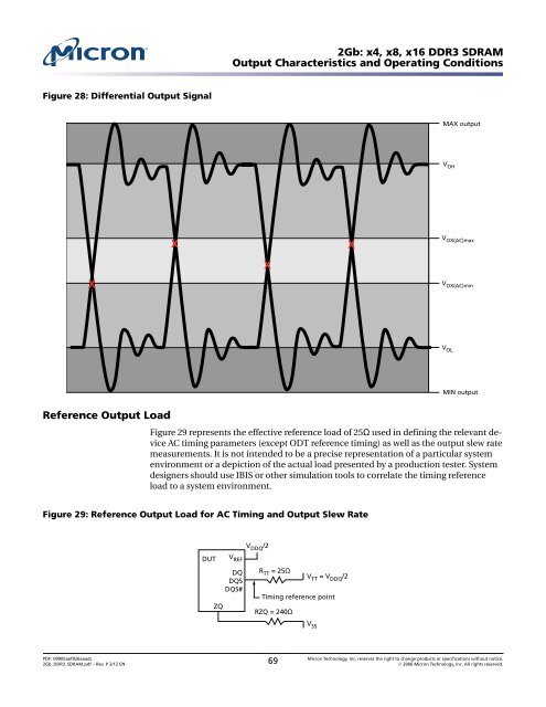
- Page 67: Output Characteristics and Operatin
- Page 71 and 72: Slew Rate Definitions for Different
- Page 73 and 74: Table 53: DDR3-1333 Speed Bins DDR3
- Page 75 and 76: Table 55: DDR3-1866 Speed Bins DDR3
- Page 77 and 78: PDF: 09005aef826aaadc Micron Techno
- Page 79 and 80: PDF: 09005aef826aaadc Micron Techno
- Page 81 and 82: PDF: 09005aef826aaadc Micron Techno
- Page 83 and 84: PDF: 09005aef826aaadc Micron Techno
- Page 85 and 86: 2Gb: x4, x8, x16 DDR3 SDRAM Electri
- Page 87 and 88: PDF: 09005aef826aaadc Micron Techno
- Page 89 and 90: PDF: 09005aef826aaadc Micron Techno
- Page 91 and 92: PDF: 09005aef826aaadc Micron Techno
- Page 93 and 94: PDF: 09005aef826aaadc Micron Techno
- Page 95 and 96: 2Gb: x4, x8, x16 DDR3 SDRAM Electri
- Page 97 and 98: 2Gb: x4, x8, x16 DDR3 SDRAM Command
- Page 99 and 100: Table 62: Derating Values for t IS/
- Page 101 and 102: Figure 32: Nominal Slew Rate and t
- Page 103 and 104: Figure 34: Tangent Line for t IS (C
- Page 105 and 106: Data Setup, Hold, and Derating 2Gb:
- Page 107 and 108: Table 68: Derating Values for t DS/
- Page 109 and 110: 2Gb: x4, x8, x16 DDR3 SDRAM Data Se
- Page 111 and 112: Figure 37: Nominal Slew Rate for t
- Page 113 and 114: Figure 39: Tangent Line for t DH (D
- Page 115 and 116: 2Gb: x4, x8, x16 DDR3 SDRAM Command
- Page 117 and 118: Commands DESELECT NO OPERATION ZQ C
- Page 119 and 120:
PRECHARGE REFRESH 2Gb: x4, x8, x16
- Page 121 and 122:
DLL Disable Mode • All other self
- Page 123 and 124:
Figure 42: DLL Disable Mode to DLL
- Page 125 and 126:
Input Clock Frequency Change 2Gb: x
- Page 127 and 128:
Write Leveling Figure 45: Write Lev
- Page 129 and 130:
Write Leveling Procedure 2Gb: x4, x
- Page 131 and 132:
Write Leveling Mode Exit Procedure
- Page 133 and 134:
Figure 48: Initialization Sequence
- Page 135 and 136:
Figure 50: MRS to nonMRS Command Ti
- Page 137 and 138:
Table 77: Burst Order Burst Length
- Page 139 and 140:
Mode Register 1 (MR1) Figure 53: Mo
- Page 141 and 142:
On-Die Termination (ODT) WRITE LEVE
- Page 143 and 144:
Mode Register 2 (MR2) Figure 55: Mo
- Page 145 and 146:
SRT versus ASR 2Gb: x4, x8, x16 DDR
- Page 147 and 148:
Figure 58: MPR Block Diagram Memory
- Page 149 and 150:
PDF: 09005aef826aaadc Micron Techno
- Page 151 and 152:
PDF: 09005aef826aaadc Micron Techno
- Page 153 and 154:
MPR Read Predefined Pattern The pre
- Page 155 and 156:
ACTIVATE Operation Before any READ
- Page 157 and 158:
READ Operation Figure 66: READ Late
- Page 159 and 160:
PDF: 09005aef826aaadc Micron Techno
- Page 161 and 162:
PDF: 09005aef826aaadc Micron Techno
- Page 163 and 164:
2Gb: x4, x8, x16 DDR3 SDRAM READ Op
- Page 165 and 166:
Figure 77: Data Strobe Timing - REA
- Page 167 and 168:
Figure 80: t RPST Timing CK CK# DQS
- Page 169 and 170:
Figure 81: t WPRE Timing Figure 82:
- Page 171 and 172:
PDF: 09005aef826aaadc Micron Techno
- Page 173 and 174:
PDF: 09005aef826aaadc Micron Techno
- Page 175 and 176:
Figure 90: WRITE (BL8) to PRECHARGE
- Page 177 and 178:
Figure 93: Data Input Timing DQS, D
- Page 179 and 180:
Figure 94: Self Refresh Entry/Exit
- Page 181 and 182:
Power-Down Mode Power-down is synch
- Page 183 and 184:
Figure 95: Active Power-Down Entry
- Page 185 and 186:
Figure 98: Power-Down Entry After R
- Page 187 and 188:
Figure 102: ACTIVATE to Power-Down
- Page 189 and 190:
RESET Operation 2Gb: x4, x8, x16 DD
- Page 191 and 192:
On-Die Termination (ODT) Figure 107
- Page 193 and 194:
Dynamic ODT Dynamic ODT Special Use
- Page 195 and 196:
Table 89: Mode Registers for R TT(W
- Page 197 and 198:
PDF: 09005aef826aaadc Micron Techno
- Page 199 and 200:
Synchronous ODT Mode ODT Latency an
- Page 201 and 202:
PDF: 09005aef826aaadc Micron Techno
- Page 203 and 204:
PDF: 09005aef826aaadc Micron Techno
- Page 205 and 206:
PDF: 09005aef826aaadc Micron Techno
- Page 207 and 208:
PDF: 09005aef826aaadc Micron Techno
- Page 209 and 210:
PDF: 09005aef826aaadc Micron Techno
- Page 211 and 212:
PDF: 09005aef826aaadc Micron Techno