

CMOS Optical Preamplifier Design Using Graphical Circuit Analysis
CMOS Optical Preamplifier Design Using Graphical Circuit Analysis
CMOS Optical Preamplifier Design Using Graphical Circuit Analysis

Create successful ePaper yourself
Turn your PDF publications into a flip-book with our unique Google optimized e-Paper software.
that<br />
and the port impedance is given by<br />
Z port<br />
i p<br />
4.4 Determining Port Impedances 94<br />
(4.13)<br />
(4.14)<br />
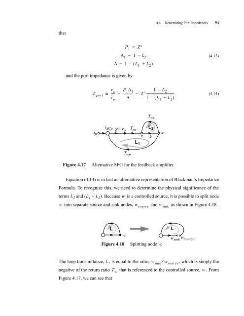
Equation (4.14) is in fact an alternative representation of Blackman’s Impedance<br />
Formula. To recognize this, we need to determine the physical significance of the<br />
terms L2 and (L1 + L2 ). Because w is a controlled source, it is possible to split node<br />
w into separate source and sink nodes, wsource and wsink as shown in Figure 4.18.<br />
The loop transmittance, L, is equal to the ratio, wsink ⁄ wsource, which is simply the<br />
negative of the return ratio that is referenced to the controlled source, w<br />
. From<br />
Figure 4.17, we can see that<br />
≡<br />
v p<br />
----<br />
i p<br />
P 1<br />
=<br />
Z°<br />
∆1 = 1 – L2 ∆ = 1 – ( L1 + L2) i SCp v p<br />
P1∆1 1 – L2 = ------------ = Z° ----------------------------------<br />
∆ 1 – ( L1 + L2) Z o<br />
T wp<br />
Tpx<br />
Figure 4.17 Alternative SFG for the feedback amplifier.<br />
L 1<br />
x<br />
T wx<br />
L 2<br />
L L<br />
w<br />
Figure 4.18 Splitting node w.<br />
T w<br />
k<br />
w<br />
wsink wsource


