

CMOS Optical Preamplifier Design Using Graphical Circuit Analysis
CMOS Optical Preamplifier Design Using Graphical Circuit Analysis
CMOS Optical Preamplifier Design Using Graphical Circuit Analysis

You also want an ePaper? Increase the reach of your titles
YUMPU automatically turns print PDFs into web optimized ePapers that Google loves.
3.3 A Low-Voltage Transimpedance Amplifier 68<br />
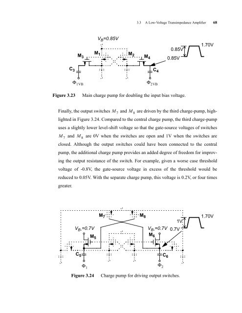
Figure 3.23 Main charge pump for doubling the input bias voltage.<br />
Finally, the output switches and are driven by the third charge-pump, high-<br />
lighted in Figure 3.24. Compared to the central charge pump, the third charge-pump<br />
uses a slightly lower level-shift voltage so that the gate-source voltages of switches<br />
M 7<br />
C 3<br />
and are 0V when the switches are open and 1V when the switches are<br />
closed. Although the output switches could have been connected to the central<br />
pump, the additional charge pump provides an added degree of freedom for improv-<br />
ing the output resistance of the switch. For example, given a worse case threshold<br />
voltage of -0.8V, the gate-source voltage in excess of the threshold would be<br />
reduced to 0.05V. With the separate charge pump, this voltage is 0.2V, or four times<br />
greater.<br />
M 3<br />
Φ 1VB<br />
M 8<br />
V B- =0.7V<br />
C 5<br />
Φ 1<br />
M 5<br />
M 1<br />
V B =0.85V<br />
M 7<br />
M 7<br />
M 2<br />
M 8<br />
M 8<br />
M 4<br />
C 4<br />
Φ 2VB<br />
V B- =0.7V<br />
M 6<br />
Φ 2<br />
C 6<br />
0.85V<br />
0.85V<br />
Figure 3.24 Charge pump for driving output switches.<br />
1V<br />
0.7V<br />
1.70V<br />
1.70V


