

CMOS Optical Preamplifier Design Using Graphical Circuit Analysis
CMOS Optical Preamplifier Design Using Graphical Circuit Analysis
CMOS Optical Preamplifier Design Using Graphical Circuit Analysis

You also want an ePaper? Increase the reach of your titles
YUMPU automatically turns print PDFs into web optimized ePapers that Google loves.
4.5 Analyzing Transistor <strong>Circuit</strong>s 103<br />
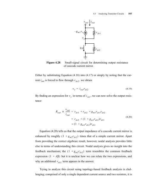
Either by substituting Equation (4.18) into (4.17) or simply by noting that the cur-<br />
rent i out is forced to flow through , we obtain<br />
(4.19)<br />
By finding an expression for in terms of , we can now solve the output resis-<br />
tance<br />
– gm1v<br />
x<br />
0A<br />
(4.20)<br />
Equation (4.20) tells us that the output impedance of a cascode current mirror is<br />
enhanced by roughly ( 1 + gm2r ds2)<br />
times that of a simple current mirror. Apart<br />
from providing the correct algebraic result, however, nodal analysis provides little<br />
else in terms of understanding this circuit. Nodal analysis gives no insight into the<br />
feedback mechanism; the ( 1 + gm2r ds2)<br />
term resembles the common feedback<br />
expression ( 1 + Aβ)<br />
but it is unclear how we can relate the two expressions, and<br />
why an additional term appears in the answer.<br />
v x<br />
Trying to analyze this circuit using topology-based feedback analysis is chal-<br />
lenging; comprised of only a single dependent current source and two resistors, it is<br />
v out<br />
i out<br />
r ds1<br />
r ds2<br />
Figure 4.28 Small-signal circuit for determining output resistance<br />
of cascode current mirror.<br />
R out<br />
r ds2<br />
v x<br />
vout -------iout<br />
v x<br />
r ds2<br />
=<br />
i out r ds2<br />
i out<br />
≡ = rds1 + rds2 + gm1r ds1rds2 = rds2 + ( 1 + gm1r ds2)rds1<br />
≈ ( 1 + gm1r ds2)rds1


