

CMOS Optical Preamplifier Design Using Graphical Circuit Analysis
CMOS Optical Preamplifier Design Using Graphical Circuit Analysis
CMOS Optical Preamplifier Design Using Graphical Circuit Analysis

You also want an ePaper? Increase the reach of your titles
YUMPU automatically turns print PDFs into web optimized ePapers that Google loves.
3.3 A Low-Voltage Transimpedance Amplifier 69<br />
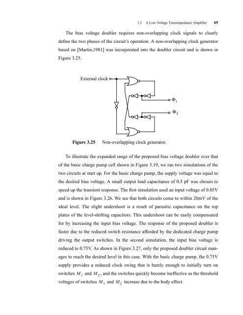
The bias voltage doubler requires non-overlapping clock signals to clearly<br />
define the two phases of the circuit’s operation. A non-overlapping clock generator<br />
based on [Martin,1981] was incorporated into the doubler circuit and is shown in<br />
Figure 3.25.<br />
Figure 3.25 Non-overlapping clock generator.<br />
To illustrate the expanded range of the proposed bias voltage doubler over that<br />
of the basic charge pump cell shown in Figure 3.19, we ran two simulations of the<br />
two circuits at start up. For the basic charge pump, the supply voltage was equal to<br />
the desired bias voltage. A small output load capacitance of 0.5 pF was chosen to<br />
speed up the transient response. The first simulation used an input voltage of 0.85V<br />
and is shown in Figure 3.26. We see that both circuits come to within 20mV of the<br />
ideal level. The slight undershoot is a result of parasitic capacitance on the top<br />
plates of the level-shifting capacitors. This undershoot can be easily compensated<br />
for by increasing the input bias voltage. The response of the proposed doubler is<br />
faster due to the reduced switch resistance afforded by the dedicated charge pump<br />
driving the output switches. In the second simulation, the input bias voltage is<br />
reduced to 0.75V. As shown in Figure 3.27, only the proposed doubler circuit man-<br />
ages to reach the desired level in this case. With the basic charge pump, the 0.75V<br />
supply provides a reduced clock swing that is barely enough to initially turn on<br />
M 1<br />
External clock<br />
switches and , and the switches quickly become ineffective as the threshold<br />
M 2<br />
voltages of switches and increase due to the body effect.<br />
M 1<br />
M 2<br />
Φ 1<br />
Φ 2


