

CMOS Optical Preamplifier Design Using Graphical Circuit Analysis
CMOS Optical Preamplifier Design Using Graphical Circuit Analysis
CMOS Optical Preamplifier Design Using Graphical Circuit Analysis

Create successful ePaper yourself
Turn your PDF publications into a flip-book with our unique Google optimized e-Paper software.
i in<br />
5.1 <strong>Analysis</strong> of the Low-Voltage Transimpedance Amplifier 110<br />
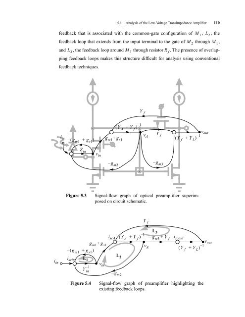
feedback that is associated with the common-gate configuration of M 1, L2 , the<br />
feedback loop that extends from the input terminal to the gate of through ,<br />
and L3 , the feedback loop around M 3 through resistor R f . The presence of overlapping<br />
feedback loops makes this structure difficult for analysis using conventional<br />
feedback techniques.<br />
i in<br />
– ( + )<br />
g m1<br />
Z in<br />
g s1<br />
v in<br />
( + ) 1 –<br />
Y A<br />
gm1 + gs1 – gm2 Y f<br />
Y f<br />
Y f<br />
M 2<br />
vA ( Y f + Y L)<br />
1 –<br />
– gm3 Figure 5.3 Signal-flow graph of optical preamplifier superimposed<br />
on circuit schematic.<br />
– ( +<br />
gm1 + gs1 )<br />
i scin<br />
g m1<br />
L 1<br />
g s1<br />
– 1<br />
Y in<br />
v in<br />
i scA<br />
( + ) 1 –<br />
L 2<br />
– gm2 Y A<br />
Y f<br />
Figure 5.4 Signal-flow graph of preamplifier highlighting the<br />
existing feedback loops.<br />
Y f<br />
L3 – gm3 + Y f<br />
i scout<br />
v out<br />
vA ( Y f + Y L)<br />
1 –<br />
v out<br />
M 1


