

CMOS Optical Preamplifier Design Using Graphical Circuit Analysis
CMOS Optical Preamplifier Design Using Graphical Circuit Analysis
CMOS Optical Preamplifier Design Using Graphical Circuit Analysis

Create successful ePaper yourself
Turn your PDF publications into a flip-book with our unique Google optimized e-Paper software.
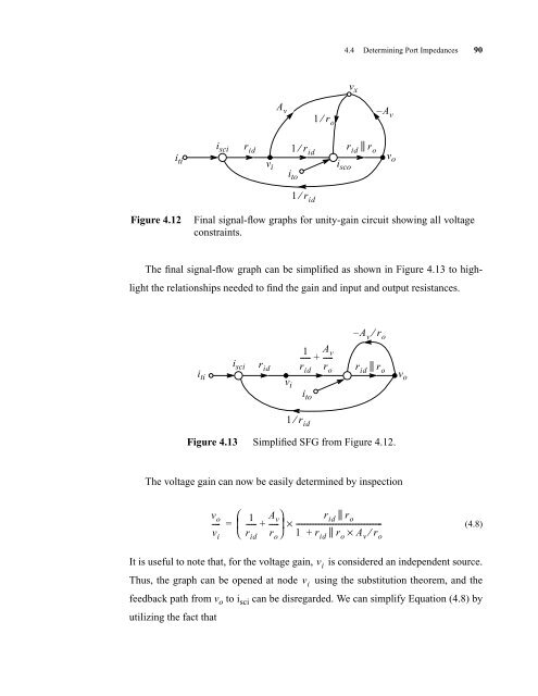
4.4 Determining Port Impedances 90<br />
Figure 4.12 Final signal-flow graphs for unity-gain circuit showing all voltage<br />
constraints.<br />
The final signal-flow graph can be simplified as shown in Figure 4.13 to high-<br />
light the relationships needed to find the gain and input and output resistances.<br />
The voltage gain can now be easily determined by inspection<br />
It is useful to note that, for the voltage gain, vi is considered an independent source.<br />
Thus, the graph can be opened at node vi using the substitution theorem, and the<br />
feedback path from vo to isci can be disregarded. We can simplify Equation (4.8) by<br />
utilizing the fact that<br />
1 ⁄ ro isci rid 1 ⁄ rid iti vi isco ito i ti<br />
i sci<br />
r id<br />
1 ⁄ rid v x<br />
A v Av<br />
v i<br />
1<br />
----- Av + -----<br />
r id<br />
r ||<br />
id ro Figure 4.13 Simplified SFG from Figure 4.12.<br />
vo ---vi<br />
r id<br />
r o<br />
i to<br />
1 ⁄ rid r o<br />
–<br />
– Av ⁄ ro r ||<br />
id ro 1<br />
----- A ⎛ v⎞<br />
r ||<br />
id ro = ⎜ + ----- ⎟ × ------------------------------------------------<br />
⎝ ⎠ 1 + r || id ro × Av ⁄ ro v o<br />
v o<br />
(4.8)


