

CMOS Optical Preamplifier Design Using Graphical Circuit Analysis
CMOS Optical Preamplifier Design Using Graphical Circuit Analysis
CMOS Optical Preamplifier Design Using Graphical Circuit Analysis

Create successful ePaper yourself
Turn your PDF publications into a flip-book with our unique Google optimized e-Paper software.
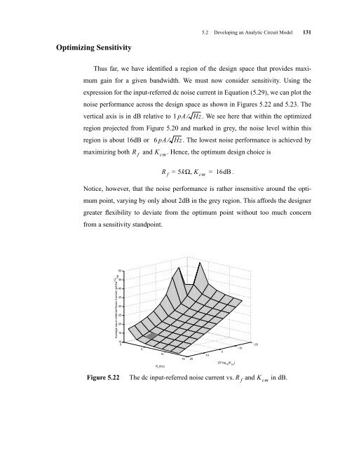
Optimizing Sensitivity<br />
5.2 Developing an Analytic <strong>Circuit</strong> Model 131<br />
Thus far, we have identified a region of the design space that provides maxi-<br />
mum gain for a given bandwidth. We must now consider sensitivity. <strong>Using</strong> the<br />
expression for the input-referred dc noise current in Equation (5.29), we can plot the<br />
noise performance across the design space as shown in Figures 5.22 and 5.23. The<br />
vertical axis is in dB relative to 1 pA ⁄ Hz.<br />
We see here that within the optimized<br />
region projected from Figure 5.20 and marked in grey, the noise level within this<br />
region is about 16dB or 6 pA ⁄ Hz.<br />
The lowest noise performance is achieved by<br />
maximizing both and . Hence, the optimum design choice is<br />
R f<br />
K cm<br />
R f = 5kΩ,<br />
K cm = 16dB .<br />
Notice, however, that the noise performance is rather insensitive around the opti-<br />
mum point, varying by only about 2dB in the grey region. This affords the designer<br />
greater flexibility to deviate from the optimum point without too much concern<br />
from a sensitivity standpoint.<br />
Average input−referred Noise Current (pA/Hz 1/2 ) dB<br />
50<br />
45<br />
40<br />
35<br />
30<br />
25<br />
20<br />
15<br />
10<br />
0<br />
5<br />
10<br />
R f (kΩ)<br />
15<br />
20<br />
10<br />
0<br />
20*log 10 (K cm )<br />
Figure 5.22 The dc input-referred noise current vs. R f and K cm<br />
in dB.<br />
−10<br />
−20


