

CMOS Optical Preamplifier Design Using Graphical Circuit Analysis
CMOS Optical Preamplifier Design Using Graphical Circuit Analysis
CMOS Optical Preamplifier Design Using Graphical Circuit Analysis

Create successful ePaper yourself
Turn your PDF publications into a flip-book with our unique Google optimized e-Paper software.
7.2 Future Work 165<br />
The significance of the DPI/SFG analysis method lies in its ability to visually<br />
represent the complex dynamics of a circuit. The signal-flow graph is complete with<br />
no simplifications, and yet it provides a framework for simplification by breaking<br />
down the complex interactions within a circuit into individual graph branches and<br />
nodes. This decomposition allows the designer to make small, isolated simplifica-<br />
tions that progressively reduce the graph until only the essential features of the cir-<br />
cuit are represented.<br />
<strong>Design</strong> is as much an art as it is a science, and ultimately the question of what<br />
design method is best rests with the designer. We have strived here to present DPI/<br />
SFG analysis clearly, and to provide enough background for the reader to learn the<br />
method in order to draw his or her own conclusions.<br />
7.2 FUTURE WORK<br />
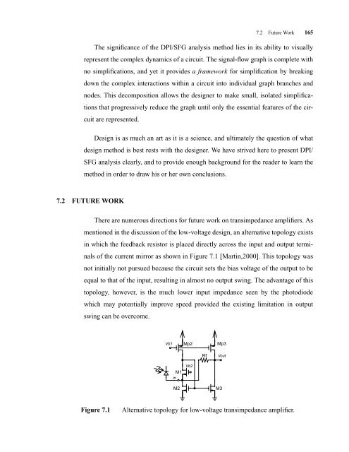
There are numerous directions for future work on transimpedance amplifiers. As<br />
mentioned in the discussion of the low-voltage design, an alternative topology exists<br />
in which the feedback resistor is placed directly across the input and output termi-<br />
nals of the current mirror as shown in Figure 7.1 [Martin,2000]. This topology was<br />
not initially not pursued because the circuit sets the bias voltage of the output to be<br />
equal to that of the input, resulting in almost no output swing. The advantage of this<br />
topology, however, is the much lower input impedance seen by the photodiode<br />
which may potentially improve speed provided the existing limitation in output<br />
swing can be overcome.<br />
Vb1<br />
Vb2<br />
M1<br />
in<br />
Mp2 Mp3<br />
Rf<br />
Vout<br />
M2 M3<br />
Figure 7.1 Alternative topology for low-voltage transimpedance amplifier.


