- Page 1 and 2:
CMOS Optical Preamplifier Design Us
- Page 3 and 4:
To achieve low-voltage operation, w
- Page 5 and 6:
Table of Contents CHAPTER 1 INTRODU
- Page 7 and 8:
CHAPTER 1 1.1 OVERVIEW Introduction
- Page 9 and 10:
Information Source Modulator Drive
- Page 11 and 12:
1.2 Thesis Outline 5 [Ohhata,1999].
- Page 13 and 14:
1.2 Thesis Outline 7 technique call
- Page 15 and 16:
1.2 Thesis Outline 9 Detector in St
- Page 17 and 18:
E e + - V bias 2.1 Photodetectors 1
- Page 19 and 20:
Diode Capacitance (pF) Diode capaci
- Page 21 and 22:
2.2 Optical Preamplifier Structures
- Page 23 and 24:
2.3 Transimpedance Amplifier Design
- Page 25 and 26:
2.3 Transimpedance Amplifier Design
- Page 27 and 28:
I dc 2.3 Transimpedance Amplifier D
- Page 29 and 30:
2.3 Transimpedance Amplifier Design
- Page 31 and 32:
Source Figure 2.11 General structur
- Page 33 and 34:
A = = For = 1V , the solution is v
- Page 35 and 36:
The gain of the forward amplifier c
- Page 37 and 38:
Feedback Analysis Using Return Rati
- Page 39 and 40:
2.4 Circuit Analysis Techniques 33
- Page 41 and 42:
2.5 An Overview of Signal-Flow Grap
- Page 43 and 44:
1 x1 x2 2.5 An Overview of Signal-F
- Page 45 and 46:
2.6 SUMMARY REFERENCES • ∆ k =
- Page 47 and 48:
Symp. Circuits Systems, vol. 3, pp.
- Page 49 and 50:
CHAPTER 3 New Transimpedance Amplif
- Page 51 and 52:
3.1 A Differential Transimpedance A
- Page 53 and 54:
3.1 A Differential Transimpedance A
- Page 55 and 56:
3.1 A Differential Transimpedance A
- Page 57 and 58:
3.2 A Feedback Topology for Ambient
- Page 59 and 60:
3.2 A Feedback Topology for Ambient
- Page 61 and 62:
Transimpedance (dBΩ) 90 80 60 40
- Page 63 and 64:
3.3 A Low-Voltage Transimpedance Am
- Page 65 and 66:
3.3 A Low-Voltage Transimpedance Am
- Page 67 and 68:
3.3 A Low-Voltage Transimpedance Am
- Page 69 and 70:
3.3 A Low-Voltage Transimpedance Am
- Page 71 and 72:
3.3 A Low-Voltage Transimpedance Am
- Page 73 and 74:
C 3 Φ1VB M 3 V B- =0.7V M 7 Figure
- Page 75 and 76:
3.3 A Low-Voltage Transimpedance Am
- Page 77 and 78:
3.4 SUMMARY 3.4 Summary 71 In this
- Page 79 and 80:
3.4 Summary 73 Y. Nakagome et al.,
- Page 81 and 82:
4.1 Introduction 75 back topology o
- Page 83 and 84:
4.2 Circuit Analysis Using Driving-
- Page 85 and 86:
4.2 Circuit Analysis Using Driving-
- Page 87 and 88:
4.2 Circuit Analysis Using Driving-
- Page 89 and 90:
4.2 Circuit Analysis Using Driving-
- Page 91 and 92:
4.3 DPI/SFG: Combining DPI Analysis
- Page 93 and 94:
4.4 Determining Port Impedances 87
- Page 95 and 96: v i R in v o R out 4.4 Determining
- Page 97 and 98: id » ro and 1 ⁄ rid « Av ⁄ ro
- Page 99 and 100: 4.4 Determining Port Impedances 93
- Page 101 and 102: 4.4 Determining Port Impedances 95
- Page 103 and 104: Z b r e g m 4.5 Analyzing Transisto
- Page 105 and 106: 4.5 Analyzing Transistor Circuits 9
- Page 107 and 108: Figure 4.25 SFG for the source foll
- Page 109 and 110: 4.5 Analyzing Transistor Circuits 1
- Page 111 and 112: 4.5 Analyzing Transistor Circuits 1
- Page 113 and 114: 4.5 Analyzing Transistor Circuits 1
- Page 115 and 116: 5.1 Analysis of the Low-Voltage Tra
- Page 117 and 118: 5.1 Analysis of the Low-Voltage Tra
- Page 119 and 120: 5.2 DEVELOPING AN ANALYTIC CIRCUIT
- Page 121 and 122: Z in 5.2 Developing an Analytic Cir
- Page 123 and 124: 5.2 Developing an Analytic Circuit
- Page 125 and 126: I n1 : i in I n2 -I n1 i scin ( sCi
- Page 127 and 128: 5.2 Developing an Analytic Circuit
- Page 129 and 130: I nRf : 5.2 Developing an Analytic
- Page 131 and 132: DC transimpedance gain: Pole locati
- Page 133 and 134: Frequency (MHz) 500 450 400 350 300
- Page 135 and 136: Pole frequencies(MHz) 500 450 400 3
- Page 137 and 138: Optimizing Sensitivity 5.2 Developi
- Page 139 and 140: 5.2 Developing an Analytic Circuit
- Page 141 and 142: Transimpedance Volts dB (lin) Gain
- Page 143 and 144: CHAPTER 6 Implementation and Experi
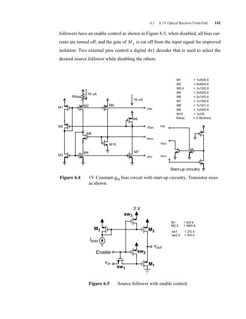
- Page 145: 6.1 A 1V Optical Receiver Front-End
- Page 149 and 150: 6.1.2 Experimental Results 6.1 A 1V
- Page 151 and 152: Gain(dB) 0 −1 −2 −3 −4 −5
- Page 153 and 154: 6.1 A 1V Optical Receiver Front-End
- Page 155 and 156: 6.1 A 1V Optical Receiver Front-End
- Page 157 and 158: 6.1 A 1V Optical Receiver Front-End
- Page 159 and 160: Clock signal of voltage doubler Eye
- Page 161 and 162: 6.2 Variable-Gain Transimpedance Am
- Page 163 and 164: 6.2.2 Experimental Results 6.2 Vari
- Page 165 and 166: 6.3 Summary and State-of-the-Art Co
- Page 167 and 168: Reference Outputs Technology Supply
- Page 169 and 170: CHAPTER 7 Conclusions 7.1 SUMMARY A
- Page 171 and 172: 7.2 Future Work 165 The significanc
- Page 173 and 174: 7.2 Future Work 167 supply and subs
- Page 175 and 176: v s i ti that part of the SFG for Q
- Page 177 and 178: Thus, P1 ′ = b = 500Ω ∆1 ′
- Page 179 and 180: itive representation of circuit dyn
- Page 181 and 182: Bipolar Transistor i scb Z b v b b