

CMOS Optical Preamplifier Design Using Graphical Circuit Analysis
CMOS Optical Preamplifier Design Using Graphical Circuit Analysis
CMOS Optical Preamplifier Design Using Graphical Circuit Analysis

Create successful ePaper yourself
Turn your PDF publications into a flip-book with our unique Google optimized e-Paper software.
4.5 Analyzing Transistor <strong>Circuit</strong>s 102<br />
recognizing the feedback can be traced to the unintended use of the Source Absorp-<br />
tion Theorem. <strong>Using</strong> this theorem has the unfortunate consequence of hiding the<br />
feedback because the transconductance element which feeds back a current in<br />
response to a voltage is represented only as a resistance. DPI/SFG analysis allows<br />
us to make a distinction, in essence bringing out lost details in the circuit’s opera-<br />
tion.<br />
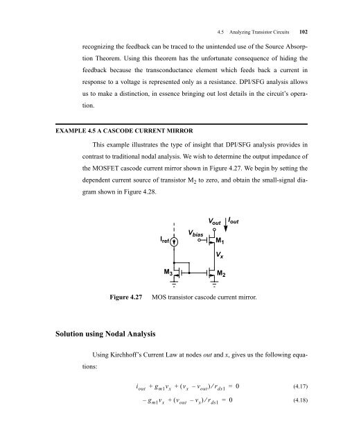
EXAMPLE 4.5 A CASCODE CURRENT MIRROR<br />
This example illustrates the type of insight that DPI/SFG analysis provides in<br />
contrast to traditional nodal analysis. We wish to determine the output impedance of<br />
the MOSFET cascode current mirror shown in Figure 4.27. We begin by setting the<br />
dependent current source of transistor M 2 to zero, and obtain the small-signal dia-<br />
gram shown in Figure 4.28.<br />
Solution using Nodal <strong>Analysis</strong><br />
tions:<br />
I ref<br />
V bias<br />
V out<br />
<strong>Using</strong> Kirchhoff’s Current Law at nodes out and x, gives us the following equa-<br />
M 1<br />
V x<br />
M 3 M2<br />
I out<br />
Figure 4.27 MOS transistor cascode current mirror.<br />
iout + gm1v x + ( vx – vout) ⁄ rds1 = 0<br />
– gm1v x + ( vout – vx) ⁄ rds1 =<br />
0<br />
(4.17)<br />
(4.18)


