

CMOS Optical Preamplifier Design Using Graphical Circuit Analysis
CMOS Optical Preamplifier Design Using Graphical Circuit Analysis
CMOS Optical Preamplifier Design Using Graphical Circuit Analysis

Create successful ePaper yourself
Turn your PDF publications into a flip-book with our unique Google optimized e-Paper software.
v i<br />
R in<br />
v o<br />
R out<br />
4.4 Determining Port Impedances 89<br />
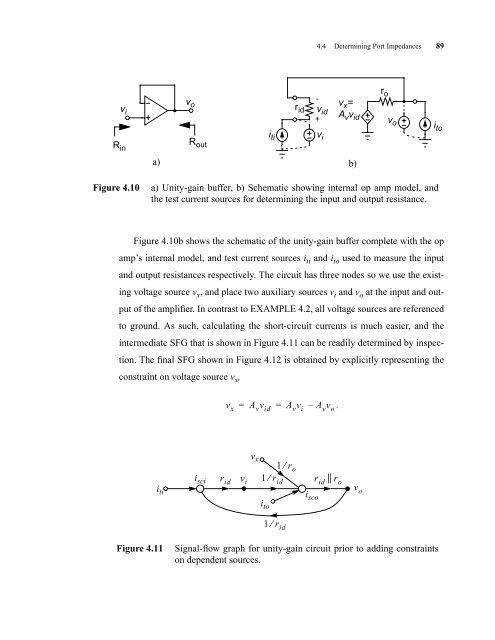
Figure 4.10b shows the schematic of the unity-gain buffer complete with the op<br />
amp’s internal model, and test current sources i ti and i to used to measure the input<br />
and output resistances respectively. The circuit has three nodes so we use the exist-<br />
ing voltage source v x , and place two auxiliary sources v i and v o at the input and out-<br />
put of the amplifier. In contrast to EXAMPLE 4.2, all voltage sources are referenced<br />
to ground. As such, calculating the short-circuit currents is much easier, and the<br />
intermediate SFG that is shown in Figure 4.11 can be readily determined by inspec-<br />
tion. The final SFG shown in Figure 4.12 is obtained by explicitly representing the<br />
constraint on voltage source v x ,<br />
i ti<br />
-<br />
rid vid<br />
+<br />
v i<br />
vx =<br />
Avvid a) b)<br />
Figure 4.10 a) Unity-gain buffer, b) Schematic showing internal op amp model, and<br />
the test current sources for determining the input and output resistance.<br />
vx = Avvid = Avvi – Avvo 1 ⁄ ro iti isci rid vi 1 ⁄<br />
rid r || id ro isco v x<br />
i to<br />
1 ⁄ rid Figure 4.11 Signal-flow graph for unity-gain circuit prior to adding constraints<br />
on dependent sources.<br />
.<br />
v o<br />
r o<br />
v o<br />
i to


