

CMOS Optical Preamplifier Design Using Graphical Circuit Analysis
CMOS Optical Preamplifier Design Using Graphical Circuit Analysis
CMOS Optical Preamplifier Design Using Graphical Circuit Analysis

Create successful ePaper yourself
Turn your PDF publications into a flip-book with our unique Google optimized e-Paper software.
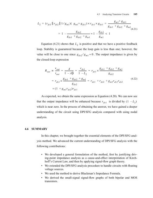
4.5 Analyzing Transistor <strong>Circuit</strong>s 105<br />
Equation (4.21) shows that is positive and that we have a positive feedback<br />
loop. Stability is guaranteed because the loop gain is less than one; however, the<br />
value will be close to one since gds2 ⁄ gm1 ≈ 0 . The output impedance is given by<br />
the closed-loop expression<br />
(4.22)<br />
As expected, we obtain the same expression as Equation (4.20). We can now see<br />
that the output impedance will be enhanced because rds1 is divided by ( 1 – L2) which is near zero. In the process of obtaining the answer, we have gained a deeper<br />
understanding of the circuit using DPI/SFG analysis compared with using nodal<br />
analysis.<br />
4.6 SUMMARY<br />
gm1+ gds1 L2 = ( r ||<br />
ds1 r ||<br />
ds2 1 ⁄ gm1) ( gm1+ gds1) × rds1 × gds1 = --------------------------------------------gds1<br />
+ gds2 + gm1 (4.21)<br />
R out<br />
≡<br />
v out<br />
--------<br />
i out<br />
r ds1<br />
In this chapter, we brought together the essential elements of the DPI/SFG anal-<br />
ysis method. We advanced the current understanding of DPI/SFG analysis with the<br />
following contributions:<br />
g ds2<br />
g ds2<br />
= 1 – --------------------------------------------- ≈ 1 – --------- < 1<br />
gds1 + gds2 + gm1 gm1 L 2<br />
A rds1 gds1 + gds2 + gm1 = ----------------- = --------------- = rds1 × ---------------------------------------------<br />
1 – Aβ 1 – L2 gds2 gds1 + gds2 + gm1 = × --------------------------------------------- = rds1 + rds2 + gm1r ds1rds2 g ds2<br />
≈ ( 1 + gm1r ds2)rds1<br />
• We developed a general formulation of the method, first by justifying driving-point<br />
impedance analysis as a cause-and-effect interpretation of Kirchhoff’s<br />
Current Law, and then by applying signal-flow graph theory.<br />
• We extended the DPI/SFG analysis procedure to handle circuits with floating<br />
voltage sources.<br />
• We used the method to derive Blackman’s Impedance Formula.<br />
• We derived the small-signal signal-flow graphs of both bipolar and MOS<br />
transistors.


