

CMOS Optical Preamplifier Design Using Graphical Circuit Analysis
CMOS Optical Preamplifier Design Using Graphical Circuit Analysis
CMOS Optical Preamplifier Design Using Graphical Circuit Analysis

You also want an ePaper? Increase the reach of your titles
YUMPU automatically turns print PDFs into web optimized ePapers that Google loves.
3.3 A Low-Voltage Transimpedance Amplifier 57<br />
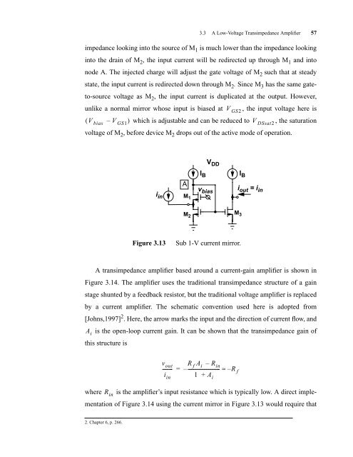
impedance looking into the source of M 1 is much lower than the impedance looking<br />
into the drain of M 2 , the input current will be redirected up through M 1 and into<br />
node A. The injected charge will adjust the gate voltage of M 2 such that at steady<br />
state, the input current is redirected down through M 2 . Since M 3 has the same gate-<br />
to-source voltage as M 2 , the input current is duplicated at the output. However,<br />
unlike a normal mirror whose input is biased at , the input voltage here is<br />
( V bias – V GS1)<br />
which is adjustable and can be reduced to V DSsat2 , the saturation<br />
voltage of M2 , before device M2 drops out of the active mode of operation.<br />
A transimpedance amplifier based around a current-gain amplifier is shown in<br />
Figure 3.14. The amplifier uses the traditional transimpedance structure of a gain<br />
stage shunted by a feedback resistor, but the traditional voltage amplifier is replaced<br />
by a current amplifier. The schematic convention used here is adopted from<br />
[Johns,1997] 2 . Here, the arrow marks the input and the direction of current flow, and<br />
A i<br />
is the open-loop current gain. It can be shown that the transimpedance gain of<br />
this structure is<br />
R in<br />
where is the amplifier’s input resistance which is typically low. A direct imple-<br />
mentation of Figure 3.14 using the current mirror in Figure 3.13 would require that<br />
2. Chapter 6, p. 266.<br />
i in<br />
A<br />
M 1<br />
M 2<br />
I B<br />
v bias<br />
V DD<br />
V GS2<br />
M 3<br />
Figure 3.13 Sub 1-V current mirror.<br />
v out<br />
--------<br />
i in<br />
R f Ai – Rin = – --------------------------- ≈ – R f<br />
1 + Ai I B<br />
i out = i in


