CMOS Optical Preamplifier Design Using Graphical Circuit Analysis
CMOS Optical Preamplifier Design Using Graphical Circuit Analysis
CMOS Optical Preamplifier Design Using Graphical Circuit Analysis
Create successful ePaper yourself
Turn your PDF publications into a flip-book with our unique Google optimized e-Paper software.
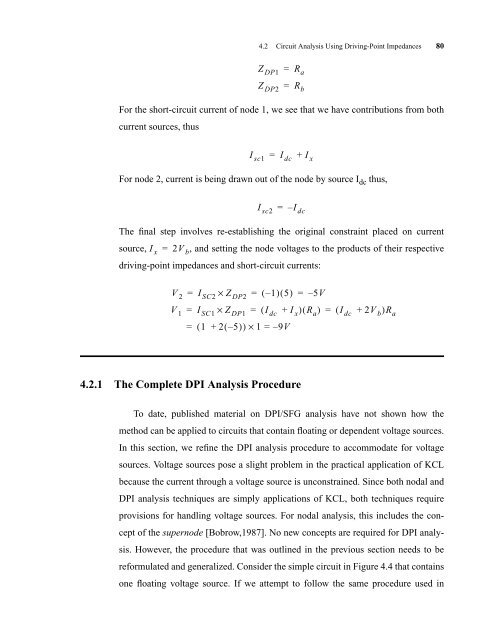
4.2 <strong>Circuit</strong> <strong>Analysis</strong> <strong>Using</strong> Driving-Point Impedances 80<br />
For the short-circuit current of node 1, we see that we have contributions from both<br />
current sources, thus<br />
Z DP1<br />
Z DP2<br />
For node 2, current is being drawn out of the node by source I dc thus,<br />
The final step involves re-establishing the original constraint placed on current<br />
source, I x = 2V b,<br />
and setting the node voltages to the products of their respective<br />
driving-point impedances and short-circuit currents:<br />
4.2.1 The Complete DPI <strong>Analysis</strong> Procedure<br />
To date, published material on DPI/SFG analysis have not shown how the<br />
method can be applied to circuits that contain floating or dependent voltage sources.<br />
In this section, we refine the DPI analysis procedure to accommodate for voltage<br />
sources. Voltage sources pose a slight problem in the practical application of KCL<br />
because the current through a voltage source is unconstrained. Since both nodal and<br />
DPI analysis techniques are simply applications of KCL, both techniques require<br />
provisions for handling voltage sources. For nodal analysis, this includes the con-<br />
cept of the supernode [Bobrow,1987]. No new concepts are required for DPI analy-<br />
sis. However, the procedure that was outlined in the previous section needs to be<br />
reformulated and generalized. Consider the simple circuit in Figure 4.4 that contains<br />
one floating voltage source. If we attempt to follow the same procedure used in<br />
=<br />
=<br />
R a<br />
R b<br />
I sc1 = I dc + I x<br />
I sc2<br />
=<br />
– I dc<br />
V 2 = I SC2 × Z DP2 = ( – 1)<br />
( 5)<br />
= – 5V<br />
V 1 = I SC1 × Z DP1 = ( I dc + I x)<br />
( Ra) = ( I dc + 2V b)Ra<br />
=<br />
( 1 + 2( – 5)<br />
) × 1 = – 9V


