

CMOS Optical Preamplifier Design Using Graphical Circuit Analysis
CMOS Optical Preamplifier Design Using Graphical Circuit Analysis
CMOS Optical Preamplifier Design Using Graphical Circuit Analysis

You also want an ePaper? Increase the reach of your titles
YUMPU automatically turns print PDFs into web optimized ePapers that Google loves.
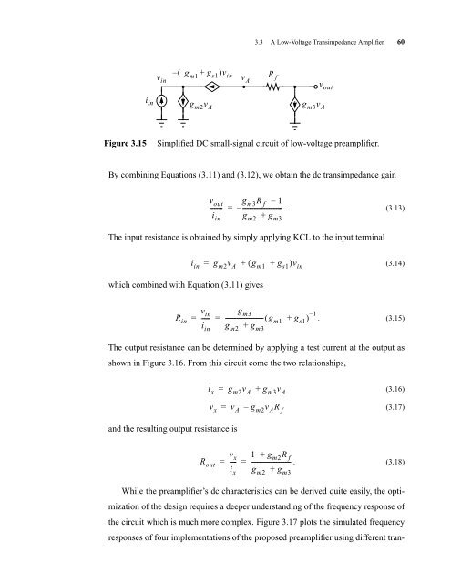
i in<br />
v in<br />
– ( gm1 + gs1)vin g m2 v A<br />
3.3 A Low-Voltage Transimpedance Amplifier 60<br />
By combining Equations (3.11) and (3.12), we obtain the dc transimpedance gain<br />
The input resistance is obtained by simply applying KCL to the input terminal<br />
which combined with Equation (3.11) gives<br />
(3.14)<br />
The output resistance can be determined by applying a test current at the output as<br />
shown in Figure 3.16. From this circuit come the two relationships,<br />
and the resulting output resistance is<br />
vA<br />
g m3 v A<br />
Figure 3.15 Simplified DC small-signal circuit of low-voltage preamplifier.<br />
R in<br />
v out<br />
--------<br />
i in<br />
(3.16)<br />
(3.17)<br />
vx 1 + gm2 R f<br />
Rout = ---- =<br />
-------------------------- . (3.18)<br />
ix gm2 + gm3 While the preamplifier’s dc characteristics can be derived quite easily, the opti-<br />
mization of the design requires a deeper understanding of the frequency response of<br />
the circuit which is much more complex. Figure 3.17 plots the simulated frequency<br />
responses of four implementations of the proposed preamplifier using different tran-<br />
R f<br />
v out<br />
gm3 R f – 1<br />
= – -------------------------- . (3.13)<br />
gm2 + gm3 iin = gm2v A + ( gm1 + gs1)vin vin gm3 ----- ------------------------- ( gm1 + gs1) . (3.15)<br />
gm2 + gm3 1 –<br />
= =<br />
i in<br />
ix = gm2v A + gm3v A<br />
vx = vA – gm2v AR f


