

CMOS Optical Preamplifier Design Using Graphical Circuit Analysis
CMOS Optical Preamplifier Design Using Graphical Circuit Analysis
CMOS Optical Preamplifier Design Using Graphical Circuit Analysis

Create successful ePaper yourself
Turn your PDF publications into a flip-book with our unique Google optimized e-Paper software.
Information<br />
Source<br />
Modulator<br />
Drive<br />
<strong>Circuit</strong>ry<br />
LED or<br />
Laser<br />
<strong>Optical</strong> channel<br />
Photodetector<br />
<strong>Preamplifier</strong><br />
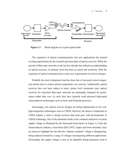
Figure 1.1 Block diagram of a typical optical link.<br />
Demodulator<br />
Transmitter Receiver<br />
1.1 Overview 3<br />
The expansion of optical communications into new applications has created<br />
exciting opportunities for the research and innovation of optical receivers. While the<br />
growth of fiber-optic networks in the last few decades has refined our understanding<br />
of optical receivers, its primary focus has been on speed and sensitivity. With the<br />
expansion of optical communications comes new requirements on receiver designs.<br />
Probably the most widespread trend has been that of increased system integra-<br />
tion and the drive to reduce system components, cost, and size. Traditionally, optical<br />
receivers have not been subject to many system level constraints since optical<br />
receivers for long-haul fiber-optic networks are principally designed for perfor-<br />
mance rather than cost. As such, they have typically used advanced high-speed<br />
semiconductor technologies such as GaAs and Si bipolar processes.<br />
Recovered<br />
Information<br />
Increasingly, new optical receiver designs are being implemented in low-cost,<br />
high-integration technologies such as <strong>CMOS</strong>. However, the desire to implement in<br />
<strong>CMOS</strong> implies a need to design receivers that keep pace with developments in<br />
<strong>CMOS</strong> technology. One of the dominant trends is the continual reduction of system<br />
supply voltage as illustrated by the forecasted trend shown in Figure 1.2 from the<br />
Semiconductor Industry Association [SIA,1997]. Upper and lower boundary lines<br />
are drawn to highlight the fact that the ‘industry standard’ voltage is disappearing,<br />
being replaced instead by a range of voltages encompassing different applications.<br />
Increasingly, the supply voltage is seen as an adaptable design parameter used to


