

CMOS Optical Preamplifier Design Using Graphical Circuit Analysis
CMOS Optical Preamplifier Design Using Graphical Circuit Analysis
CMOS Optical Preamplifier Design Using Graphical Circuit Analysis

You also want an ePaper? Increase the reach of your titles
YUMPU automatically turns print PDFs into web optimized ePapers that Google loves.
I dc<br />
2.3 Transimpedance Amplifier <strong>Design</strong> Requirements 21<br />
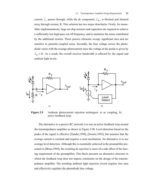
current, , passes through, while the dc component, , is blocked and shunted<br />
away through resistor, R. This solution has two major drawbacks. Firstly, for mono-<br />
lithic implementations, large on-chip resistors and capacitors are required to achieve<br />
a sufficiently low high-pass cut-off frequency, and to minimize the noise contributed<br />
by the additional resistor. These passive elements occupy significant area and are<br />
sensitive to parasitic-coupled noise. Secondly, the bias voltage across the photo-<br />
diode varies with the average photocurrent since the voltage at the anode is given by<br />
I dc × R<br />
. As a result, the overall receiver bandwidth is affected by the signal and<br />
ambient light levels.<br />
R<br />
i s<br />
i s<br />
R f<br />
v out<br />
Figure 2.9 Ambient photocurrent rejection techniques: a) ac coupling, b)<br />
active feedback loop.<br />
I dc<br />
The alternative to a passive RCnetwork is to use an active feedback loop around<br />
the transimpedance amplifier as shown in Figure 2.9b. Level detection based on the<br />
peaks of the signal is effective [Tanabe,1998], [Swartz,1993], but assumes that the<br />
average current is constant and requires a reset mechanism. An alternative is to use<br />
average level detection. Although this is essentially achieved in the preamplifier pre-<br />
sented in [Brass,1994], the resulting dc rejection is more of a side effect of the bias-<br />
ing requirement of the preamplifier. This thesis presents an alternative structure in<br />
which the feedback loop does not impose constraints on the design of the transim-<br />
pedance amplifier. The resulting ambient light rejection circuit requires less area<br />
and effectively regulates the photodiode bias voltage.<br />
I dc<br />
a) b)<br />
i s<br />
R f<br />
Level<br />
Detect<br />
v out


