

CMOS Optical Preamplifier Design Using Graphical Circuit Analysis
CMOS Optical Preamplifier Design Using Graphical Circuit Analysis
CMOS Optical Preamplifier Design Using Graphical Circuit Analysis

Create successful ePaper yourself
Turn your PDF publications into a flip-book with our unique Google optimized e-Paper software.
Pole frequencies(MHz)<br />
500<br />
450<br />
400<br />
350<br />
300<br />
250<br />
200<br />
150<br />
100<br />
50<br />
5.2 Developing an Analytic <strong>Circuit</strong> Model 129<br />
Since the process of optimizing the frequency response involves maximizing the<br />
gain for a desired bandwidth, the gain-bandwidth (GBW) product is a useful figure<br />
of merit because it combines gain and bandwidth into a single quantity. Although<br />
bandwidth and gain can be traded off with feedback, the product of the two is often<br />
fixed for a given topology, bias condition, etc. We can optimize our preamplifier<br />
design through maximizing the GBW. By approximating the bandwidth with ω p1 ,<br />
we can obtain an analytic expression for the GBW from Equations (5.25) and<br />
(5.26):<br />
0<br />
0 5<br />
R (kΩ)<br />
f<br />
10 15<br />
500<br />
450<br />
400<br />
350<br />
300<br />
250<br />
200<br />
150<br />
100<br />
0<br />
20<br />
Figure 5.20 shows the resulting 3-dimensional plot of GBW versus and<br />
(5.30)<br />
while Figure 5.21 presents the same surface in two, 2-dimensional projections<br />
views. Across the design space, we see that the GBW can vary by over an order of<br />
magnitude. We can identify that portion of the design space which meets our band-<br />
width requirement by projecting the bounded region identified in Figure 5.18 onto<br />
the GBW plot. Within this region, we have marked in grey a sub-region that corre-<br />
sponds to an area with the highest GBW.<br />
Pole frequencies(MHz)<br />
50<br />
10<br />
0 −10<br />
20*log (K )<br />
10 cm<br />
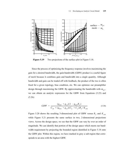
Figure 5.19 Two projections of the surface plot in Figure 5.18.<br />
GBW<br />
( gm1 + gs1) ( 1 – gm3 R f )<br />
= ----------------------------------------------------------------------------------------------<br />
Cin + ( gm1 + gs1) ( CL + C f )Rf⁄ K cm<br />
−20<br />
surface —<br />
mesh —<br />
R f<br />
ω p1<br />
ωo K cm


