

CMOS Optical Preamplifier Design Using Graphical Circuit Analysis
CMOS Optical Preamplifier Design Using Graphical Circuit Analysis
CMOS Optical Preamplifier Design Using Graphical Circuit Analysis

Create successful ePaper yourself
Turn your PDF publications into a flip-book with our unique Google optimized e-Paper software.
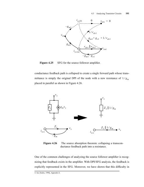
Figure 4.25 SFG for the source follower amplifier.<br />
4.5 Analyzing Transistor <strong>Circuit</strong>s 101<br />
conductance feedback path is collapsed to create a single forward path whose trans-<br />
mittance is simply the original DPI of the node with a new resistance of<br />
placed in parallel as shown in Figure 4.26.<br />
i scx<br />
Z 1<br />
v x<br />
One of the common challenges of analyzing the source follower amplifier is recog-<br />
nizing that feedback exists in the amplifier. With DPI/SFG analysis, the feedback is<br />
explicitly represented in the SFG. Moreover, we have shown that this difficulty in<br />
4. See [Sedra, 1998], Appendix E.<br />
v in<br />
– gm1<br />
g m1<br />
Z 1 v x<br />
- g m<br />
g m v x<br />
i scD1<br />
i scout<br />
0<br />
1 ⁄ rds1 gm1 + gs1 + 1 ⁄ rds1 r || ds1 rds2 - gm1– gs1 i scx<br />
v D1<br />
v out<br />
=<br />
0<br />
Z ||<br />
1 1 ⁄ gm Z || 1 1 ⁄ gm Figure 4.26 The source absorption theorem: collapsing a transconductance<br />
feedback path into a resistance.<br />
v x<br />
v x<br />
1 ⁄ gm


