

CMOS Optical Preamplifier Design Using Graphical Circuit Analysis
CMOS Optical Preamplifier Design Using Graphical Circuit Analysis
CMOS Optical Preamplifier Design Using Graphical Circuit Analysis

You also want an ePaper? Increase the reach of your titles
YUMPU automatically turns print PDFs into web optimized ePapers that Google loves.
6.1.2 Experimental Results<br />
6.1 A 1V <strong>Optical</strong> Receiver Front-End 143<br />
A micrograph of the fabricated test chip is shown in Figure 6.8. The chip measures<br />
1.0mm × 1.6mm and occupies an active area of 0.13mm . The main signal<br />
2<br />
path runs through the centre of the chip, from left to right. The bias voltage doubler<br />
was placed in the far lower corner, away from the output buffer and output driver to<br />
minimize noise coupled through parasitics.<br />
The power consumption of the 1V front-end circuit is 1mW. The power con-<br />
sumption of the 3V test circuitry is 45mW, and is essentially due to the output<br />
buffer. An external 1pF capacitor was used to model the photodiode during electri-<br />
cal testing, while a Mitel 1A354 PIN photodiode was used to construct the actual<br />
optical link. The typical capacitance of the photodiode is 1pF for a bias voltage of<br />
1V or more.<br />
Frequency Response Measurements<br />
In-<br />
Vbias<br />
M5<br />
3 V<br />
M1 M2<br />
30 uA<br />
M3 M4<br />
In+<br />
Iout<br />
M1,2 = 5/0.8<br />
M3,4 = 10/0.6<br />
M5 = 20/0.8<br />
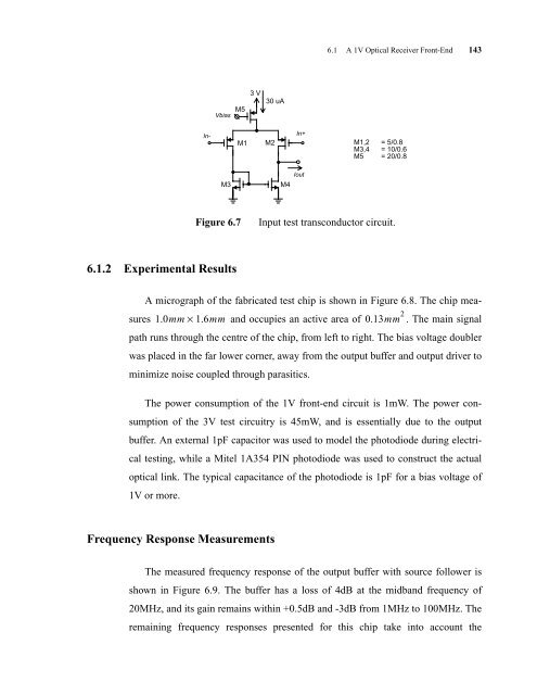
Figure 6.7 Input test transconductor circuit.<br />
The measured frequency response of the output buffer with source follower is<br />
shown in Figure 6.9. The buffer has a loss of 4dB at the midband frequency of<br />
20MHz, and its gain remains within +0.5dB and -3dB from 1MHz to 100MHz. The<br />
remaining frequency responses presented for this chip take into account the


