

CMOS Optical Preamplifier Design Using Graphical Circuit Analysis
CMOS Optical Preamplifier Design Using Graphical Circuit Analysis
CMOS Optical Preamplifier Design Using Graphical Circuit Analysis

You also want an ePaper? Increase the reach of your titles
YUMPU automatically turns print PDFs into web optimized ePapers that Google loves.
Final <strong>Design</strong><br />
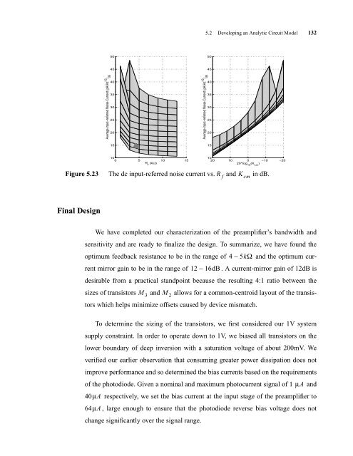
Average input−referred Noise Current (pA/Hz 1/2 ) dB<br />
50<br />
45<br />
40<br />
35<br />
30<br />
25<br />
20<br />
15<br />
10<br />
0 5<br />
R (kΩ)<br />
f<br />
10 15<br />
5.2 Developing an Analytic <strong>Circuit</strong> Model 132<br />
We have completed our characterization of the preamplifier’s bandwidth and<br />
sensitivity and are ready to finalize the design. To summarize, we have found the<br />
optimum feedback resistance to be in the range of 4 ∼ 5kΩand<br />
the optimum cur-<br />
rent mirror gain to be in the range of 12 ∼ 16dB . A current-mirror gain of 12dB is<br />
desirable from a practical standpoint because the resulting 4:1 ratio between the<br />
sizes of transistors and allows for a common-centroid layout of the transis-<br />
tors which helps minimize offsets caused by device mismatch.<br />
To determine the sizing of the transistors, we first considered our 1V system<br />
supply constraint. In order to operate down to 1V, we biased all transistors on the<br />
lower boundary of deep inversion with a saturation voltage of about 200mV. We<br />
verified our earlier observation that consuming greater power dissipation does not<br />
improve performance and so determined the bias currents based on the requirements<br />
of the photodiode. Given a nominal and maximum photocurrent signal of 1 µA and<br />
40µA respectively, we set the bias current at the input stage of the preamplifier to<br />
64 µA<br />
, large enough to ensure that the photodiode reverse bias voltage does not<br />
change significantly over the signal range.<br />
Average input−referred Noise Current (pA/Hz 1/2 ) dB<br />
50<br />
45<br />
40<br />
35<br />
30<br />
25<br />
20<br />
15<br />
10<br />
20<br />
10<br />
0 −10<br />
20*log (K )<br />
10 cm<br />
Figure 5.23 The dc input-referred noise current vs. R f and K cm in dB.<br />
M 3<br />
M 2<br />
−20


