

CMOS Optical Preamplifier Design Using Graphical Circuit Analysis
CMOS Optical Preamplifier Design Using Graphical Circuit Analysis
CMOS Optical Preamplifier Design Using Graphical Circuit Analysis

You also want an ePaper? Increase the reach of your titles
YUMPU automatically turns print PDFs into web optimized ePapers that Google loves.
4.5.2 Transistor <strong>Circuit</strong> Examples<br />
EXAMPLE 4.4 A SOURCE FOLLOWER AMPLIFIER<br />
4.5 Analyzing Transistor <strong>Circuit</strong>s 100<br />
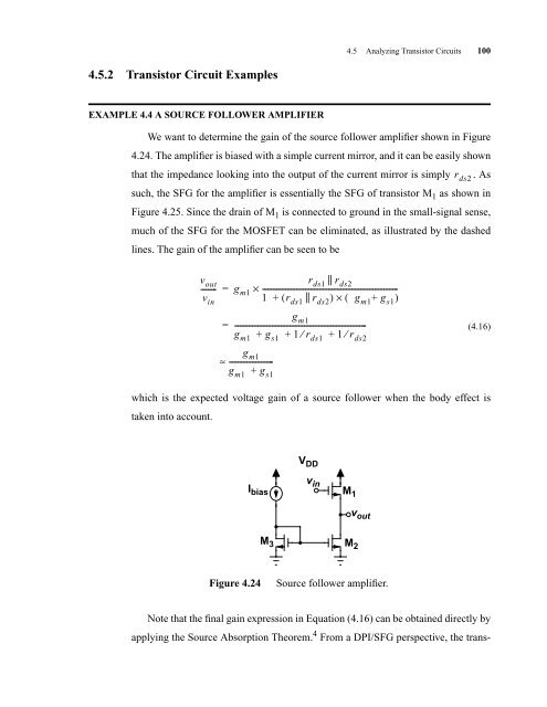
We want to determine the gain of the source follower amplifier shown in Figure<br />
4.24. The amplifier is biased with a simple current mirror, and it can be easily shown<br />
that the impedance looking into the output of the current mirror is simply . As<br />
such, the SFG for the amplifier is essentially the SFG of transistor M 1 as shown in<br />
Figure 4.25. Since the drain of M 1 is connected to ground in the small-signal sense,<br />
much of the SFG for the MOSFET can be eliminated, as illustrated by the dashed<br />
lines. The gain of the amplifier can be seen to be<br />
v in<br />
(4.16)<br />
which is the expected voltage gain of a source follower when the body effect is<br />
taken into account.<br />
vout r || ds1 rds2 -------- = gm1 × ---------------------------------------------------------------------------<br />
1 + ( r ||<br />
ds1 rds2) × ( gm1+ gs1) g m1<br />
= ------------------------------------------------------------------------gm1<br />
+ gs1 + 1 ⁄ rds1 + 1 ⁄ rds2 ≈<br />
gm1 -----------------------gm1<br />
+ gs1 I bias<br />
V DD<br />
v in<br />
Note that the final gain expression in Equation (4.16) can be obtained directly by<br />
applying the Source Absorption Theorem. 4 From a DPI/SFG perspective, the trans-<br />
M 1<br />
M 3 M2<br />
v out<br />
Figure 4.24 Source follower amplifier.<br />
r ds2


