

CMOS Optical Preamplifier Design Using Graphical Circuit Analysis
CMOS Optical Preamplifier Design Using Graphical Circuit Analysis
CMOS Optical Preamplifier Design Using Graphical Circuit Analysis

Create successful ePaper yourself
Turn your PDF publications into a flip-book with our unique Google optimized e-Paper software.
1 ⁄ sC ||<br />
in 1 ⁄ ( gm1 + gs1) ( sCin + gm1 + gs1 ) 1 –<br />
or<br />
i in<br />
i scin<br />
v in<br />
i scA<br />
gm1 + gs1 – gm2 ( + ) 1 –<br />
Y A<br />
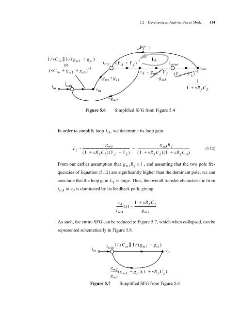
Figure 5.6 Simplified SFG from Figure 5.4<br />
In order to simplify loop , we determine its loop gain<br />
L 3<br />
5.2 Developing an Analytic <strong>Circuit</strong> Model 114<br />
(5.12)<br />
From our earlier assumption that gm3 R f » 1 , and assuming that the two pole frequencies<br />
of Equation (5.12) are significantly higher than the dominant pole, we can<br />
conclude that the loop gain is large. Thus, the overall transfer characteristic from<br />
i scA to v A is dominated by its feedback path, giving<br />
L 3<br />
As such, the entire SFG can be reduced to Figure 5.7, which when collapsed, can be<br />
represented schematically in Figure 5.8.<br />
Y f<br />
Y f<br />
1<br />
L 3<br />
i scout<br />
v out<br />
vA ( Y f + Y L)<br />
1 –<br />
– gm3 + Y f<br />
– gm3 1<br />
---------------------------<br />
1 + sRf CL – gm3 – gm3 R f<br />
≈ ----------------------------------------------------------- = ------------------------------------------------------------------<br />
( 1 + sRf CL) ( Y f + Y L)<br />
( 1 + sRf CL) ( 1 + sRf C A)<br />
i in<br />
L 3<br />
i scin<br />
vA 1 + sRf CL -------- ( s)<br />
≈ ---------------------------<br />
i scA<br />
g m3<br />
1 ⁄ sC || in 1 ⁄ ( gm1 + gs1) g m2<br />
g m3<br />
v in<br />
– -------- ( gm1 + gs1) ( 1 + sRf CL) Figure 5.7 Simplified SFG from Figure 5.6


