

3D Time-of-flight distance measurement with custom - Universität ...
3D Time-of-flight distance measurement with custom - Universität ...
3D Time-of-flight distance measurement with custom - Universität ...

You also want an ePaper? Increase the reach of your titles
YUMPU automatically turns print PDFs into web optimized ePapers that Google loves.
DEMODULATION PIXELS IN CMOS/CCD 127<br />
sinusoidal rather than square shaped input signal, the measured amplitude is<br />
attenuated to 64%, independently <strong>of</strong> the actual demodulation performance <strong>of</strong> the<br />
pixels. We do not make this correction, for two reasons: (1) We use exactly the<br />
same LEDs (HPWT-DH00, 630 nm) modulated at 20 MHz for the range cameras<br />
introduced in Chapter 6. The contrast values presented in Section 5.2.3 - 5.2.5<br />
therefore represent the real measured contrast, including the modulation shape and<br />
modulation depth <strong>of</strong> the optical input signal. And (2), as can be seen from<br />
Figure 5.12, for 20 MHz modulation the optical signal is not exactly a sinusoidal<br />
wave so that an amplitude correction by 56.25%, which corresponds to the pure<br />
sinusoidal wave, would not be absolutely correct.<br />
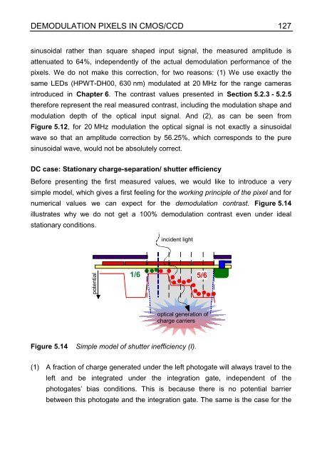
DC case: Stationary charge-separation/ shutter efficiency<br />
Before presenting the first measured values, we would like to introduce a very<br />
simple model, which gives a first feeling for the working principle <strong>of</strong> the pixel and for<br />
numerical values we can expect for the demodulation contrast. Figure 5.14<br />
illustrates why we do not get a 100% demodulation contrast even under ideal<br />
stationary conditions.<br />
potential<br />
incident light<br />
1/6 5/6<br />
optical generation <strong>of</strong><br />
charge carriers<br />
Figure 5.14 Simple model <strong>of</strong> shutter inefficiency (I).<br />
(1) A fraction <strong>of</strong> charge generated under the left photogate will always travel to the<br />
left and be integrated under the integration gate, independent <strong>of</strong> the<br />
photogates’ bias conditions. This is because there is no potential barrier<br />
between this photogate and the integration gate. The same is the case for the


