

3D Time-of-flight distance measurement with custom - Universität ...
3D Time-of-flight distance measurement with custom - Universität ...
3D Time-of-flight distance measurement with custom - Universität ...

You also want an ePaper? Increase the reach of your titles
YUMPU automatically turns print PDFs into web optimized ePapers that Google loves.
156 CHAPTER 6<br />
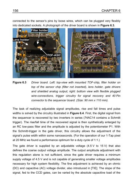
connected to the sensor’s pins by loose wires, which can be plugged very flexibly<br />
into dedicated sockets. A photograph <strong>of</strong> the driver board is shown in Figure 6.3.<br />
Lens holder<br />
Filter holder<br />
TOF-ASIC<br />
Figure 6.3 Driver board. Left: top-view <strong>with</strong> mounted TOF-chip, filter holder on<br />
top <strong>of</strong> the sensor chip (filter not inserted), lens holder, gate drivers<br />
and shielded analog output; right: bottom view <strong>with</strong> flexible plugged<br />
wire-connections, trigger circuitry for signal recovery and 40 Pin<br />
connector to the sequencer board. (Size: 90 mm x 110 mm).<br />
The task <strong>of</strong> realizing adjustable signal amplitudes, rise and fall times and pulse<br />
widths is solved by the circuitry illustrated in Figure 6.4. First, the digital signal from<br />
the sequencer is recovered by two inverters in series (74AC14 contains a Schmitt<br />
trigger). The rise/fall time <strong>of</strong> the recovered signal is then synthetically enlarged by<br />
an RC low-pass filter and the amplitude is adjusted by the potentiometer P1. With<br />
the Schmitt-trigger in the gate driver, this circuitry allows the adjustment <strong>of</strong> the<br />
signal’s pulse width <strong>with</strong>in some nanoseconds. (For the operation <strong>of</strong> our 1-Tap pixel<br />
at 20 MHz we found a performance optimum for a duty cycle <strong>of</strong> 1:1.)<br />
The gate driver is supplied by an adjustable voltage (4.5 V to 15 V) that also<br />
defines the coarse output voltage amplitude. The output amplitude adjustment <strong>with</strong><br />
this regulation alone is not sufficient, since the gate driver requires a minimum<br />
supply voltage <strong>of</strong> 4.5 V and is not capable <strong>of</strong> generating smaller voltage amplitudes<br />
necessary for high system flexibility. The fine adjustment is achieved by an ohmic<br />
(DC) and capacitive (AC) voltage divider, also introduced in [TIE]. The slope <strong>of</strong> the<br />
signal, fed to the CCD gates, can be varied by the absolute capacitive load <strong>of</strong> the


