

3D Time-of-flight distance measurement with custom - Universität ...
3D Time-of-flight distance measurement with custom - Universität ...
3D Time-of-flight distance measurement with custom - Universität ...

You also want an ePaper? Increase the reach of your titles
YUMPU automatically turns print PDFs into web optimized ePapers that Google loves.
148 CHAPTER 5<br />
When we implemented the 1-tap pixel realization, we considered implementing at<br />
least point (1) (2-tap instead <strong>of</strong> 1-tap pixel), since it is obvious that the photocharge<br />
that we currently dump <strong>with</strong> the 1-tap pixel corresponds exactly to the 180° shifted<br />
sampling point. However, we preferred at that early time to implement the easiest<br />
demodulation pixel in order to get a reliable demonstrator, rather than running the<br />
risk <strong>of</strong> receiving non-functional devices from the foundry by trying to implement too<br />
much functionality at a time.<br />
storage 0°<br />
Mod0°<br />
PGM<br />
Mod180°<br />
storage 180°<br />
CCDsep<br />
storage 90°<br />
Mod90°<br />
PGM<br />
Mod270°<br />
storage 270°<br />
0°/180°<br />
90°/270°<br />
Light sensitive<br />
(detection and<br />
demodulation)<br />
Opaque (storage)<br />
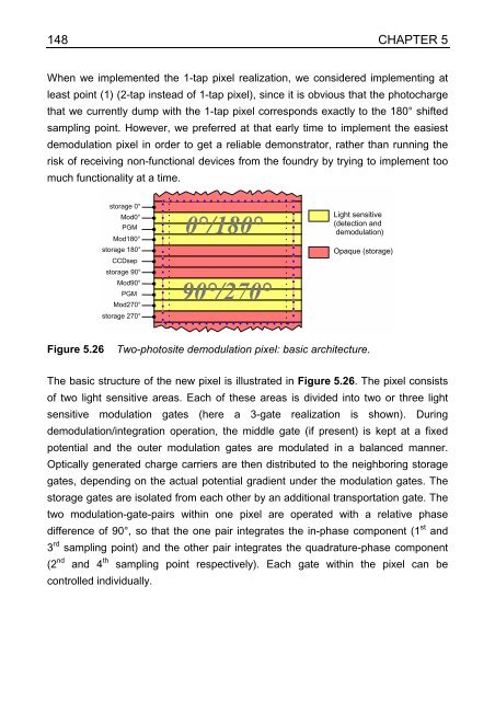
Figure 5.26 Two-photosite demodulation pixel: basic architecture.<br />
The basic structure <strong>of</strong> the new pixel is illustrated in Figure 5.26. The pixel consists<br />
<strong>of</strong> two light sensitive areas. Each <strong>of</strong> these areas is divided into two or three light<br />
sensitive modulation gates (here a 3-gate realization is shown). During<br />
demodulation/integration operation, the middle gate (if present) is kept at a fixed<br />
potential and the outer modulation gates are modulated in a balanced manner.<br />
Optically generated charge carriers are then distributed to the neighboring storage<br />
gates, depending on the actual potential gradient under the modulation gates. The<br />
storage gates are isolated from each other by an additional transportation gate. The<br />
two modulation-gate-pairs <strong>with</strong>in one pixel are operated <strong>with</strong> a relative phase<br />
difference <strong>of</strong> 90°, so that the one pair integrates the in-phase component (1 st and<br />
3 rd sampling point) and the other pair integrates the quadrature-phase component<br />
(2 nd and 4 th sampling point respectively). Each gate <strong>with</strong>in the pixel can be<br />
controlled individually.


