- Page 1 and 2:
3D Time-of-flight distance measurem
- Page 3 and 4:
To my parents
- Page 5 and 6:
Meinen Eltern
- Page 7 and 8:
II 4. Power budget and resolution l
- Page 10 and 11:
Abstract Since we are living in a t
- Page 12:
centimeter accuracy. With the singl
- Page 15 and 16:
X Eine elegantere Methode zur Entfe
- Page 18 and 19:
INTRODUCTION 1 1. Introduction One
- Page 20 and 21:
INTRODUCTION 3 light source observe
- Page 22 and 23:
INTRODUCTION 5 Propagation time, ho
- Page 24 and 25:
INTRODUCTION 7 Chapter 3 gives a sh
- Page 26 and 27:
OPTICAL TOF RANGE MEASUREMENT 9 2.
- Page 28 and 29:
OPTICAL TOF RANGE MEASUREMENT 11 2.
- Page 30 and 31:
OPTICAL TOF RANGE MEASUREMENT 13 pr
- Page 32 and 33:
OPTICAL TOF RANGE MEASUREMENT 15 hi
- Page 34 and 35:
OPTICAL TOF RANGE MEASUREMENT 17 Pu
- Page 36 and 37:
OPTICAL TOF RANGE MEASUREMENT 19 Ad
- Page 38 and 39:
OPTICAL TOF RANGE MEASUREMENT 21 pr
- Page 40 and 41:
OPTICAL TOF RANGE MEASUREMENT 23 wh
- Page 42 and 43:
OPTICAL TOF RANGE MEASUREMENT 25 δ
- Page 44 and 45:
OPTICAL TOF RANGE MEASUREMENT 27 c(
- Page 46 and 47:
OPTICAL TOF RANGE MEASUREMENT 29 A
- Page 48 and 49:
OPTICAL TOF RANGE MEASUREMENT 31 ph
- Page 50 and 51:
OPTICAL TOF RANGE MEASUREMENT 33 Ts
- Page 52 and 53:
OPTICAL TOF RANGE MEASUREMENT 35 f1
- Page 54 and 55:
OPTICAL TOF RANGE MEASUREMENT 37 an
- Page 56 and 57:
OPTICAL TOF RANGE MEASUREMENT 39 in
- Page 58 and 59:
OPTICAL TOF RANGE MEASUREMENT 41 Ss
- Page 60 and 61:
OPTICAL TOF RANGE MEASUREMENT 43 Fr
- Page 62 and 63:
OPTICAL TOF RANGE MEASUREMENT 45 1
- Page 64:
OPTICAL TOF RANGE MEASUREMENT 47 2.
- Page 67 and 68:
50 CHAPTER 3 the smearing effect, r
- Page 69 and 70:
52 CHAPTER 3 3.1 Silicon properties
- Page 71 and 72:
54 CHAPTER 3 (a) Figure 3.3 Optical
- Page 73 and 74:
56 CHAPTER 3 Quantum efficiency in
- Page 75 and 76:
58 CHAPTER 3 The different operatio
- Page 77 and 78:
60 CHAPTER 3 (a) (b) Depletion widt
- Page 79 and 80:
62 CHAPTER 3 Very special processes
- Page 81 and 82:
64 CHAPTER 3 1 kT Dn = ⋅ vth ⋅
- Page 83 and 84:
66 CHAPTER 3 The proportionality fa
- Page 85 and 86:
68 CHAPTER 3 difference of only 1 V
- Page 87 and 88:
70 CHAPTER 3 Flicker noise is cause
- Page 89 and 90:
72 CHAPTER 3 A s = sf ⋅ q C ⎡ V
- Page 91 and 92:
74 CHAPTER 3 amount of the charge p
- Page 93 and 94:
76 CHAPTER 3 substrate (Equation 3.
- Page 95 and 96:
78 CHAPTER 3 charge carriers the CT
- Page 97 and 98:
80 CHAPTER 3 without causing short
- Page 99 and 100:
82 CHAPTER 3 Over an address decode
- Page 101 and 102:
84 CHAPTER 3 Orbit’s 2.0µm CMOS/
- Page 103 and 104:
86 CHAPTER 4 Figure 4.1 P lens Lamb
- Page 105 and 106:
88 CHAPTER 4 Required optical power
- Page 107 and 108:
90 CHAPTER 4 4.2 Noise limitation o
- Page 109 and 110:
92 CHAPTER 4 number of pseudo-backg
- Page 111 and 112:
94 CHAPTER 4 Cmod = 1 QE(λ) = 0.65
- Page 113 and 114:
96 CHAPTER 4 Range accuracy (std) i
- Page 116 and 117:
DEMODULATION PIXELS IN CMOS/CCD 99
- Page 118 and 119:
DEMODULATION PIXELS IN CMOS/CCD 101
- Page 120 and 121:
DEMODULATION PIXELS IN CMOS/CCD 103
- Page 122 and 123:
DEMODULATION PIXELS IN CMOS/CCD 105
- Page 124 and 125:
DEMODULATION PIXELS IN CMOS/CCD 107
- Page 126 and 127:
DEMODULATION PIXELS IN CMOS/CCD 109
- Page 128 and 129:
DEMODULATION PIXELS IN CMOS/CCD 111
- Page 130 and 131:
DEMODULATION PIXELS IN CMOS/CCD 113
- Page 132 and 133:
DEMODULATION PIXELS IN CMOS/CCD 115
- Page 134 and 135:
DEMODULATION PIXELS IN CMOS/CCD 117
- Page 136 and 137:
DEMODULATION PIXELS IN CMOS/CCD 119
- Page 138 and 139:
DEMODULATION PIXELS IN CMOS/CCD 121
- Page 140 and 141:
DEMODULATION PIXELS IN CMOS/CCD 123
- Page 142 and 143:
DEMODULATION PIXELS IN CMOS/CCD 125
- Page 144 and 145:
DEMODULATION PIXELS IN CMOS/CCD 127
- Page 146 and 147:
DEMODULATION PIXELS IN CMOS/CCD 129
- Page 148 and 149:
DEMODULATION PIXELS IN CMOS/CCD 131
- Page 150 and 151:
DEMODULATION PIXELS IN CMOS/CCD 133
- Page 152 and 153: DEMODULATION PIXELS IN CMOS/CCD 135
- Page 154 and 155: DEMODULATION PIXELS IN CMOS/CCD 137
- Page 156 and 157: DEMODULATION PIXELS IN CMOS/CCD 139
- Page 158 and 159: DEMODULATION PIXELS IN CMOS/CCD 141
- Page 160 and 161: DEMODULATION PIXELS IN CMOS/CCD 143
- Page 162 and 163: DEMODULATION PIXELS IN CMOS/CCD 145
- Page 164 and 165: DEMODULATION PIXELS IN CMOS/CCD 147
- Page 166 and 167: DEMODULATION PIXELS IN CMOS/CCD 149
- Page 168 and 169: IMAGING TOF RANGE CAMERAS 151 6. Im
- Page 170 and 171: IMAGING TOF RANGE CAMERAS 153 contr
- Page 172 and 173: IMAGING TOF RANGE CAMERAS 155 6.1.2
- Page 174 and 175: IMAGING TOF RANGE CAMERAS 157 gate
- Page 176 and 177: IMAGING TOF RANGE CAMERAS 159 6.2 2
- Page 178 and 179: IMAGING TOF RANGE CAMERAS 161 n+ di
- Page 180 and 181: IMAGING TOF RANGE CAMERAS 163 pixel
- Page 182 and 183: IMAGING TOF RANGE CAMERAS 165 Power
- Page 184 and 185: IMAGING TOF RANGE CAMERAS 167 Delay
- Page 186 and 187: IMAGING TOF RANGE CAMERAS 169 6.3 3
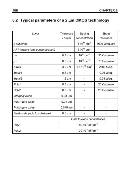
- Page 188 and 189: IMAGING TOF RANGE CAMERAS 171 Gate
- Page 190 and 191: IMAGING TOF RANGE CAMERAS 173 Bound
- Page 192 and 193: IMAGING TOF RANGE CAMERAS 175 Figur
- Page 194 and 195: IMAGING TOF RANGE CAMERAS 177 Final
- Page 196 and 197: IMAGING TOF RANGE CAMERAS 179 #5 #6
- Page 198 and 199: SUMMARY AND PERSPECTIVE 181 7. Summ
- Page 200 and 201: SUMMARY AND PERSPECTIVE 183 into th
- Page 202: SUMMARY AND PERSPECTIVE 185 or phas
- Page 207 and 208: 190 CHAPTER 8 Spectral luminous int
- Page 209 and 210: 192 CHAPTER 8 MCD03S: Conditions SC
- Page 211 and 212: 194 CHAPTER 8 MCD06S: Measurement c
- Page 213 and 214: 196 [BRK] Brockhaus, “Naturwissen
- Page 215 and 216: 198 [KAI] I. Kaisto, et al., “Opt
- Page 217 and 218: 200 [SP1] T. Spirig et al., “The
- Page 220 and 221: ACKNOWLEDGMENTS 203 Acknowledgments
- Page 222: 206 Publication list 1. R. Lange, P