

3D Time-of-flight distance measurement with custom - Universität ...
3D Time-of-flight distance measurement with custom - Universität ...
3D Time-of-flight distance measurement with custom - Universität ...

Create successful ePaper yourself
Turn your PDF publications into a flip-book with our unique Google optimized e-Paper software.
DEMODULATION PIXELS IN CMOS/CCD 149<br />
dump diffusion<br />
dump gate<br />
storage 0°<br />
Mod0°<br />
PGM<br />
Mod180°<br />
storage 180°<br />
CCDsep<br />
storage 90°<br />
Mod90°<br />
PGM<br />
Mod270°<br />
storage 270°<br />
OUT gate<br />
sense diffusion<br />
Light sensitive<br />
(detection and demodulation)<br />
adressable<br />
in-pixel APS<br />
readout circuitry<br />
0°/180°<br />
90°/270°<br />
(a)<br />
Opaque (storage)<br />
sense diffusion<br />
OUTG 0°<br />
storage 0°<br />
Mod0°<br />
PGM<br />
Mod180°<br />
storage 180°<br />
OUTG 180°<br />
sense diffusion<br />
adressable in-pixel<br />
APS readout circuitry<br />
sense diffusion<br />
OUTG 90°<br />
storage 90°<br />
Mod90°<br />
PGM<br />
Mod270°<br />
storage 270°<br />
OUTG 270°<br />
sense diffusion<br />
adressable<br />
in-pixel APS<br />
readout circuitry<br />
0°/180°<br />
90°/270°<br />
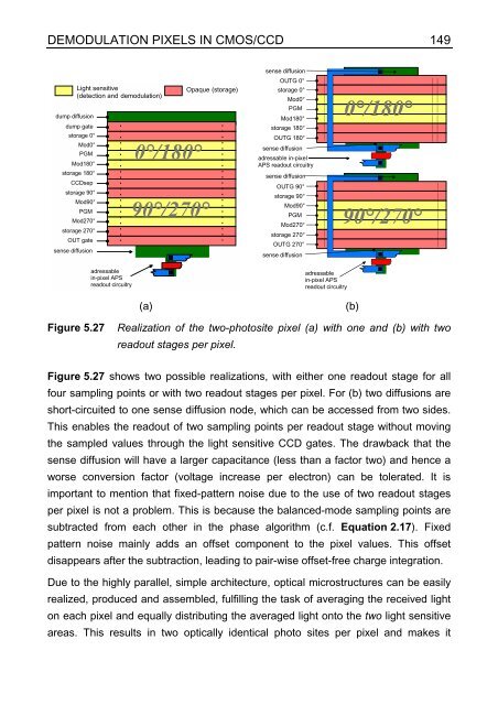
Figure 5.27 Realization <strong>of</strong> the two-photosite pixel (a) <strong>with</strong> one and (b) <strong>with</strong> two<br />
readout stages per pixel.<br />
Figure 5.27 shows two possible realizations, <strong>with</strong> either one readout stage for all<br />
four sampling points or <strong>with</strong> two readout stages per pixel. For (b) two diffusions are<br />
short-circuited to one sense diffusion node, which can be accessed from two sides.<br />
This enables the readout <strong>of</strong> two sampling points per readout stage <strong>with</strong>out moving<br />
the sampled values through the light sensitive CCD gates. The drawback that the<br />
sense diffusion will have a larger capacitance (less than a factor two) and hence a<br />
worse conversion factor (voltage increase per electron) can be tolerated. It is<br />
important to mention that fixed-pattern noise due to the use <strong>of</strong> two readout stages<br />
per pixel is not a problem. This is because the balanced-mode sampling points are<br />
subtracted from each other in the phase algorithm (c.f. Equation 2.17). Fixed<br />
pattern noise mainly adds an <strong>of</strong>fset component to the pixel values. This <strong>of</strong>fset<br />
disappears after the subtraction, leading to pair-wise <strong>of</strong>fset-free charge integration.<br />
Due to the highly parallel, simple architecture, optical microstructures can be easily<br />
realized, produced and assembled, fulfilling the task <strong>of</strong> averaging the received light<br />
on each pixel and equally distributing the averaged light onto the two light sensitive<br />
areas. This results in two optically identical photo sites per pixel and makes it<br />
(b)


