PXA3xx Design Guide - Marvell
PXA3xx Design Guide - Marvell
PXA3xx Design Guide - Marvell
- No tags were found...

You also want an ePaper? Increase the reach of your titles
YUMPU automatically turns print PDFs into web optimized ePapers that Google loves.
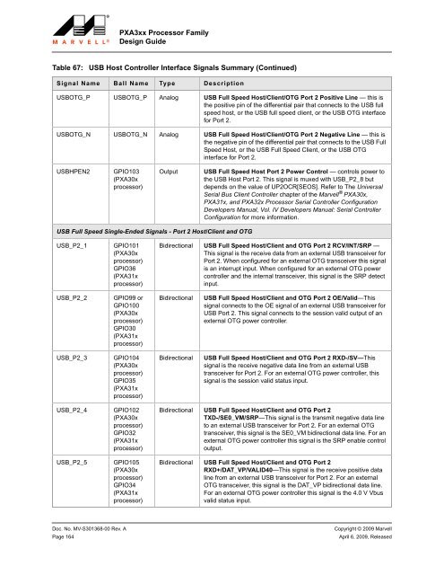
<strong>PXA3xx</strong> Processor Family<strong>Design</strong> <strong>Guide</strong>Table 67:USB Host Controller Interface Signals Summary (Continued)Signal Name Ball Name Type DescriptionUSBOTG_P USBOTG_P Analog USB Full Speed Host/Client/OTG Port 2 Positive Line — this isthe positive pin of the differential pair that connects to the USB fullspeed host, or the USB full speed client, or the USB OTG interfacefor Port 2.USBOTG_N USBOTG_N Analog USB Full Speed Host/Client/OTG Port 2 Negative Line — this isthe negative pin of the differential pair that connects to the USB FullSpeed Host, or the USB Full Speed Client, or the USB OTGinterface for Port 2.USBHPEN2GPIO103(PXA30xprocessor)OutputUSB Full Speed Host Port 2 Power Control — controls power tothe USB Host Port 2. This signal is muxed with USB_P2_8 butdepends on the value of UP2OCR[SEOS]. Refer to The UniversalSerial Bus Client Controller chapter of the <strong>Marvell</strong> ® PXA30x,PXA31x, and PXA32x Processor Serial Controller ConfigurationDevelopers Manual, Vol. IV Developers Manual: Serial ControllerConfiguration for more information.USB Full Speed Single-Ended Signals - Port 2 Host/Client and OTGUSB_P2_1GPIO101(PXA30xprocessor)GPIO36(PXA31xprocessor)Bidirectional USB Full Speed Host/Client and OTG Port 2 RCV/INT/SRP —This signal is the receive data from an external USB transceiver forPort 2. When configured for an external OTG transceiver this signalis an interrupt input. When configured for an external OTG powercontroller and the internal transceiver, this signal is the SRP detectinput.USB_P2_2GPIO99 orGPIO100(PXA30xprocessor)GPIO30(PXA31xprocessor)BidirectionalUSB Full Speed Host/Client and OTG Port 2 OE/Valid—Thissignal connects to the OE signal of an external USB transceiver forUSB Port 2. This signal connects to the session valid output of anexternal OTG power controller.USB_P2_3GPIO104(PXA30xprocessor)GPIO35(PXA31xprocessor)BidirectionalUSB Full Speed Host/Client and OTG Port 2 RXD-/SV—Thissignal is the receive negative data line from an external USBtransceiver for Port 2. For an external OTG power controller, thissignal is the session valid status input.USB_P2_4USB_P2_5GPIO102(PXA30xprocessor)GPIO32(PXA31xprocessor)GPIO105(PXA30xprocessor)GPIO34(PXA31xprocessor)Bidirectional USB Full Speed Host/Client and OTG Port 2TXD-/SE0_VM/SRP—This signal is the transmit negative data lineto an external USB transceiver for Port 2. For an external OTGtransceiver, this signal is the SE0_VM bidirectional data line. For anexternal OTG power controller this signal is the SRP enable controloutput.Bidirectional USB Full Speed Host/Client and OTG Port 2RXD+/DAT_VP/VALID40—This signal is the receive positive dataline from an external USB transceiver for Port 2. For an externalOTG transceiver, this signal is the DAT_VP bidirectional data line.For an external OTG power controller this signal is the 4.0 V Vbusvalid status input.Doc. No. MV-S301368-00 Rev. A Copyright © 2009 <strong>Marvell</strong>Page 164April 6, 2009, Released