PXA3xx Design Guide - Marvell
PXA3xx Design Guide - Marvell
PXA3xx Design Guide - Marvell
- No tags were found...

You also want an ePaper? Increase the reach of your titles
YUMPU automatically turns print PDFs into web optimized ePapers that Google loves.
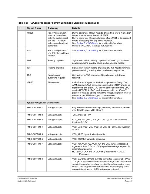
Table 85:<strong>PXA3xx</strong> Processor Family Schematic Checklist (Continued) Signal Name Category DetailsnTRSTTCKFor JTAG operation,must be driven fromboth the system resetand the JTAG toolsindependently withoutcontention.For JTAG operation,use 10K ohm pulldownresistor.During power-up, nTRST must be driven from low to high eitherbefore or at the same time as nRESET.During power-up, 10 µs must elapse after nTRST is de-assertedbefore proceeding with any JTAG operation.See Section 9, JTAG Debug for additional information.Pullup to VCC_BBATT using a 10K resistor.See Section 9, JTAG Debug for additional information.TMS Floating or pullup. Signal must remain floating or pullup (10-100 KΩ) to minimizepower use during standby, sleep, and deep sleep modes.TDI Floating or pullup Signal must remain floating or pull-up (10-100 KΩ) to minimizepower use during standby, sleep, and deep sleep modes.TDONo pullups orpulldowns requiredConnect from JTAG connector. No pull-ups or pull-downsrequired.nSRST Bidirectional nSRST is not a signal on the <strong>PXA3xx</strong> processor family. TheARM standard JTAG connector specifies the nSRST should bebidirectional and allow JTAG to both sense and drive the CPUreset (nRESET). A JTAG module connected to an XScale ®processor must be able to control the nRESET signal in order toenable proper JTAG debugger communication.See Section 9, JTAG Debug for additional information.Typical Voltage Rail ConnectionsPMIC OUTPUT 1 Voltage Supply Regulated Main battery voltage, nominally 3.0V (not to exceedmax 4.0V) to power VCC_BBATTPMIC OUTPUT 2 Voltage Supply VCC_MEM @ 1.8VPMIC OUTPUT 3 Voltage Supply VCC_BG, VCC_MVT, VCC_PLL, VCC_OSC13M connectedtogether @ 1.8VPMIC OUTPUT 4 Voltage Supply VCC_LCD, VCC_MSL, VCC_CI, VCC_DF connected togetherat 1.8VPMIC OUTPUT 5 Voltage Supply VCC_APPS dynamically adjustablePMIC OUTPUT 6 Voltage Supply VCC_SRAM dynamically adjustablePMIC OUTPUT 7 Voltage Supply VCC_IO1, VCC_IO3, VCC_IO4 and VCC_IO6 connectectedtogether at 1.8V, 3.0V or 3.3V (depends on voltage required forexternal components)NOTE: VCC_IO4 and VCCIO6 only apply to the PXA32xProcessorPMIC OUTPUT 8 Voltage Supply VCC_CARD1 and VCC_CARD2 connected together at 1.8V or3.0V (+/- 10%) to USIM or Removable storage card. This can besupplied by another regulator passing through an analog powerswitch. This supply can be connected to another supply of theappropriate voltage is USIM functions are not used.Copyright © 2009 <strong>Marvell</strong>Doc. No. MV-S301368-00 Rev. AApril 6, 2009, Released Page 207