PXA3xx Design Guide - Marvell
PXA3xx Design Guide - Marvell
PXA3xx Design Guide - Marvell
- No tags were found...
Create successful ePaper yourself
Turn your PDF publications into a flip-book with our unique Google optimized e-Paper software.
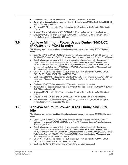
• Configure OSCC[TENS0] appropriately. This setting is system dependent.• To verify that the applications subsystem is in the D2 state use JTAG to check that ASCR[D2S]= 0b1. This step is optional.• Ensure AD2R[AD2_L2] = 0b0. This verifies that the L2 cache is in the D2 state. This step isoptional.• Ensure TDI and TMS pins and EXT_WAKEUP are pulled high or remain floating.• Ensure the USB OTG differential inputs (USBOTG_P and USBOTG_N) are driven high orremain floating with no impact to OTG pins.3.6 Achieve Minimum Power Usage During S0/D1/C2(PXA30x and PXA31x only)The following methods are used to achieve lowest power consumption during S0/D1/C2 powermode:• Set VCC_APPS and VCC_CORE to the minimum allowable voltage for S0/D1/C2 as defined inthe <strong>Marvell</strong> ® PXA30x and PXA31x Processor Electrical, Mechanical, and Thermal Specification.• Set all other power domains to their minimum possible voltage allowable by the systemconfiguration. This is dependent upon the peripherals connected to the <strong>PXA3xx</strong> processorfamily. All voltages must comply with the voltage requirements of the PXA30x and PXA31xprocessor. Refer to the <strong>Marvell</strong> ® PXA30x and PXA31x Processor Electrical, Mechanical, andThermal Specification for more information.• Clear PCFR[PUDH]. This disables the pull-up and pull-down registers for nGPIO_RESET,EXT_WAKEUP, PWR_SCL, and PWR_SDA.• Configure AD2R[AD2_Rx] appropriately for the LCD buffer in the internal SRAM. Write 0b1 foreach bank of internal SRAM that contains LCD frame buffer data and write 0b0 to all otherbanks.• Configure OSCC[TENS0] appropriately. This setting is system dependent.• To verify that the applications subsystem is in the D1 state use JTAG to verify that ASCR[D1S] =0b1. This step is optional.• Ensure AD1R[AD1_L2] = 0b0. This verifies that the L2 cache is in the D1 state. This step isoptional.• Ensure TDI and TMS pins and EXT_WAKEUP are pulled high or remain floating.• Ensure the USB OTG differential inputs (USBOTG_P and USBOTG_N) are driven high orremain floating with no impact to OTG pins.3.7 Achieve Minimum Power Usage During S0/D0CSIdleThe following are methods used to achieve lowest power consumption during S0/D0CS Idle powermode:• Set VCC_APPS and VCC_CORE to the minimum allowable voltage for S0/D0CS Idle asdefined in the <strong>Marvell</strong> ® PXA30x, PXA31x, and PXA32x Processor Electrical, Mechanical, andThermal Specification.• Set all other power domains to their minimum possible voltage allowable by the systemconfiguration. This is dependent upon the peripherals connected to the <strong>PXA3xx</strong> processorfamily. All voltages must comply with the voltage requirements of the <strong>PXA3xx</strong> processor family.Refer to the <strong>Marvell</strong> ® PXA30x, PXA31x, and PXA32x Processor Electrical, Mechanical, andThermal Specification for more information.• Clear PCFR[PUDH]. This disables the pull-up and pull-down registers for nGPIO_RESET,EXT_WAKEUP, PWR_SCL, and PWR_SDA.• Configure OSCC[TENS0] appropriately. This setting is system dependent.Copyright © 2009 <strong>Marvell</strong>Doc. No. MV-S301368-00 Rev. AApril 6, 2009, Released Page 33


