PXA3xx Design Guide - Marvell
PXA3xx Design Guide - Marvell
PXA3xx Design Guide - Marvell
- No tags were found...

You also want an ePaper? Increase the reach of your titles
YUMPU automatically turns print PDFs into web optimized ePapers that Google loves.
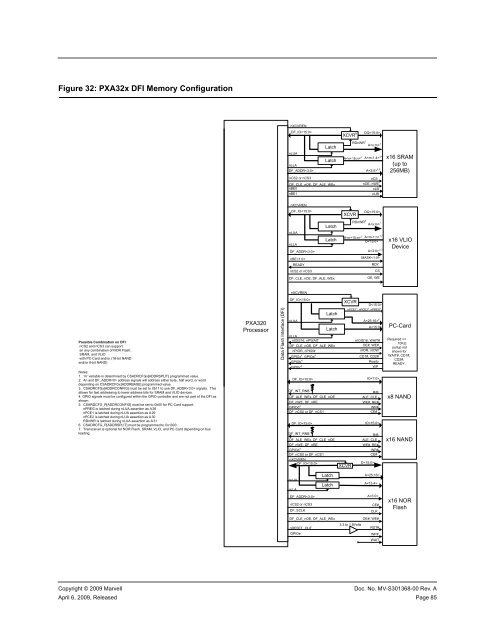
Figure 32: PXA32x DFI Memory ConfigurationnXCVRENDF_IOXCVR 9DQPossible Combination on DFInCS2 and nCS3 can supportan any combination of NOR Flash,SRAM, and VLIOwith PC-Card and/or (16-bit NANDand/or 8-bit NAND)Notes:1. ‘m’ variable is determined by CSADRCFGx[ADDRSPLIT] programmed value.2. An and DF_ADDR address signals will address either byte, half word, or worddepending on CSADRCFGx[ADDRBASE] programmed value.3. CSADRCFGx[ADDRCONFIG] must be set to 0b11 to use DF_ADDR signals. Thisallows for fast addressing to lower address bits for SRAM and VLIO devices .4 GPIO signals must be configured within the GPIO controller and are not part of the DFI asshown.5. CSARDCFG_P[ADDRCONFIG] must be set to 0b00 for PC-Card support.nPREG is latched during nLUA assertion as A 26nPCE1 is latched during nLUA assertion as A29nPCE2 is latched during nLUA assertion as A30RDnWR is latched during nLUA assertion as A 316. CSADRCFG_P[ADDRSPLIT] must be programmed to 0x1000.7. Transceiver is optional for NOR Flash, SRAM, VLIO, and PC-Card depending on busloading..PXA320ProcessorData Flash Interface (DFI)LatchRDnWR 7A 3nLUAGPIOd 4 WP#LatchA 4 A 3,4nLLADF_ADDRA 4,5nCS2 or nCS3nCSDF_CLE_nOE, DF_ALE_WExnOE, nWEnBE0nLBnBE1nUBnXCVRENDF_IOXCVRDQRDnWR 5LatchA 1nLUALatchA 2 A 1,2DnLLADF_ADDRA ,2,3nBEMASKREADYRDYnCS2 or nCS3CSDF_CLE_nOE, DF_ALE_WExOE, WEnXCVRENDF_IOXCVRDnPCE1 5 , nPCE2 5 , nPREG 5LatchnLUAA 6LatchAnLLAnIOIS16, nPWAITnIOIS16, WAIT#DF_CLE_nOE, DF_ALE_WExOE#, WE#nPIOR, nPIOWnIOR, nIOWGPIOz 4 , GPIOa 4CD1#, CD2#GPIOb 4ReadyGPIOc 4WPDF_IOIODF_INT_RNBR/BDF_ALE_WEx, DF_CLE_nOEALE, CLEDF_nWE, DF_nREWE#, RE#GPIOd 4WP#DF_nCS0 or DF_nCS1CE#DF_IOIODF_INT_RNBR/BDF_ALE_WEx, DF_CLE_nOEALE, CLEDF_nWE, DF_nREWE#, RE#DF_nCS0 or DF_nCS1CE#nXCVRENDF_IODXCVRx16 SRAM(up to256MB)x16 VLIODevicePC-CardRequired >=10KΩpullup notshown forWAIT#, CD1#,CD2#,READY,x8 NANDx16 NANDnLUAnLLALatchLatchAADF_ADDRnCS2 or nCS3DF_SCLKACE#CLKx16 NORFlashDF_CLE_nOE, DF_ALE_WExnRESET_OUTGPIOeOE#, WE#3.3 to 1.8VoltsRST#WP#WAITXCopyright © 2009 <strong>Marvell</strong>Doc. No. MV-S301368-00 Rev. AApril 6, 2009, Released Page 85