PXA3xx Design Guide - Marvell
PXA3xx Design Guide - Marvell
PXA3xx Design Guide - Marvell
- No tags were found...

You also want an ePaper? Increase the reach of your titles
YUMPU automatically turns print PDFs into web optimized ePapers that Google loves.
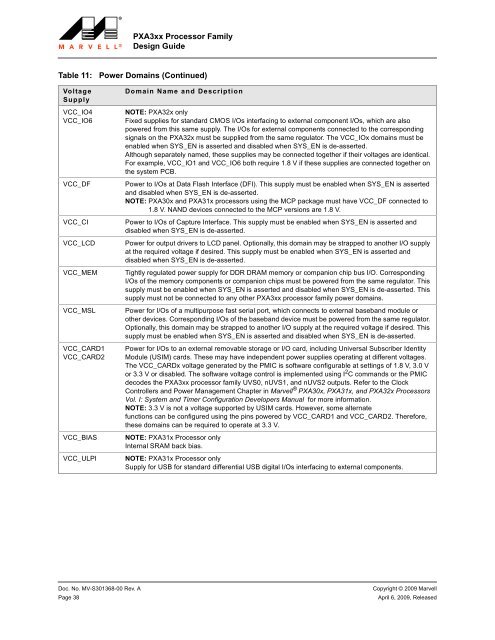
<strong>PXA3xx</strong> Processor Family<strong>Design</strong> <strong>Guide</strong>Table 11:VoltageSupplyPower Domains (Continued)Domain Name and DescriptionVCC_IO4VCC_IO6VCC_DFVCC_CIVCC_LCDVCC_MEMVCC_MSLVCC_CARD1VCC_CARD2VCC_BIASVCC_ULPINOTE: PXA32x onlyFixed supplies for standard CMOS I/Os interfacing to external component I/Os, which are alsopowered from this same supply. The I/Os for external components connected to the correspondingsignals on the PXA32x must be supplied from the same regulator. The VCC_IOx domains must beenabled when SYS_EN is asserted and disabled when SYS_EN is de-asserted.Although separately named, these supplies may be connected together if their voltages are identical.For example, VCC_IO1 and VCC_IO6 both require 1.8 V if these supplies are connected together onthe system PCB.Power to I/Os at Data Flash Interface (DFI). This supply must be enabled when SYS_EN is assertedand disabled when SYS_EN is de-asserted.NOTE: PXA30x and PXA31x processors using the MCP package must have VCC_DF connected to1.8 V. NAND devices connected to the MCP versions are 1.8 V.Power to I/Os of Capture Interface. This supply must be enabled when SYS_EN is asserted anddisabled when SYS_EN is de-asserted.Power for output drivers to LCD panel. Optionally, this domain may be strapped to another I/O supplyat the required voltage if desired. This supply must be enabled when SYS_EN is asserted anddisabled when SYS_EN is de-asserted.Tightly regulated power supply for DDR DRAM memory or companion chip bus I/O. CorrespondingI/Os of the memory components or companion chips must be powered from the same regulator. Thissupply must be enabled when SYS_EN is asserted and disabled when SYS_EN is de-asserted. Thissupply must not be connected to any other <strong>PXA3xx</strong> processor family power domains.Power for I/Os of a multipurpose fast serial port, which connects to external baseband module orother devices. Corresponding I/Os of the baseband device must be powered from the same regulator.Optionally, this domain may be strapped to another I/O supply at the required voltage if desired. Thissupply must be enabled when SYS_EN is asserted and disabled when SYS_EN is de-asserted.Power for I/Os to an external removable storage or I/O card, including Universal Subscriber IdentityModule (USIM) cards. These may have independent power supplies operating at different voltages.The VCC_CARDx voltage generated by the PMIC is software configurable at settings of 1.8 V, 3.0 Vor 3.3 V or disabled. The software voltage control is implemented using I 2 C commands or the PMICdecodes the <strong>PXA3xx</strong> processor family UVS0, nUVS1, and nUVS2 outputs. Refer to the ClockControllers and Power Management Chapter in <strong>Marvell</strong> ® PXA30x, PXA31x, and PXA32x ProcessorsVol. I: System and Timer Configuration Developers Manual for more information.NOTE: 3.3 V is not a voltage supported by USIM cards. However, some alternatefunctions can be configured using the pins powered by VCC_CARD1 and VCC_CARD2. Therefore,these domains can be required to operate at 3.3 V.NOTE: PXA31x Processor onlyInternal SRAM back bias.NOTE: PXA31x Processor onlySupply for USB for standard differential USB digital I/Os interfacing to external components.Doc. No. MV-S301368-00 Rev. A Copyright © 2009 <strong>Marvell</strong>Page 38 April 6, 2009, Released