BC-3500 Series - Rowe International
BC-3500 Series - Rowe International
BC-3500 Series - Rowe International
You also want an ePaper? Increase the reach of your titles
YUMPU automatically turns print PDFs into web optimized ePapers that Google loves.
<strong>BC</strong>-<strong>3500</strong> Bill and Coin Changer<br />
DETAILED CONTROL COMPUTER BOARD OPERATION<br />
The following description is not intended for the casual repair person or the novice technician. It details the electronics<br />
found on the control computer board. No attempt should be made to repair this board unless you have had<br />
considerable experience troubleshooting and repairing complex, microprocessor-controlled electronic circuit<br />
boards. <strong>Rowe</strong> suggests that you send any defective CCC boards back to the factory for proper servicing.<br />
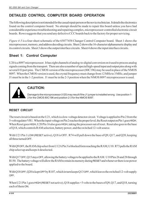
Figure 4-5 is a four-sheet schematic of the 65077458 Changer Control Computer board. Sheet 1 shows the<br />
microprocessor, memory, and address decoding circuits. Sheet 2 shows the 16-character alphanumeric display and<br />
its control circuits. Sheet 3 shows the output interface circuits. Sheet 4 shows the input interface circuits.<br />
Sheet 1: Control Computer<br />
U20 is a 8097 microprocessor. It has eight channels of analog-to-digital conversion on it used to process analog<br />
signals coming from the transport. There are also a number of special high-speed input and output pins along with<br />
several I/O port pins. The CMOS version of the microprocessor (80C196) may be used in place of the NMOS<br />
8097. When the CMOS version is used, the crystal frequency must change from 12 MHz to 3 MHz, and jumper<br />
J1 must be in the 1-2 position. J1 must be in the 2-3 position when the NMOS 8097 microprocessor is used.<br />
CAUTION:<br />
Damage to the microprocessor (V20) may result if the J1 jumper is installed wrong. Use position 1-<br />
2 for the CMOS 80C196 and position 2-3 for the NMOS 8097.<br />
RESET CIRCUIT<br />
The reset circuit is based on the U21, which is a low-voltage detector circuit. Voltage is applied to Pin 2 from the<br />
5-volt regulator VR1. When the input voltage on Pin 2 reaches the proper level, the Reset output on Pin 1 goes HIGH.<br />
When Reset goes HIGH, U20 Pin 16 also goes HIGH, taking the processor out of reset. Reset also goes to the base<br />
of Q18, which controls RAM selection, battery power, and the switched 12-volt source.<br />
With U21 Pin 1 LOW (RESET active), Q18 is OFF. R74 will pull down the base of Q9, Q17, and Q20, keeping<br />
all three turned OFF.<br />
With Q9 OFF, the RAM chip select from U12A Pin 3 is blocked form reaching the RAM, U10. R73 pulls the RAM<br />
chip select up and keeps it deselected.<br />
With Q17 OFF, Q15 stays OFF, allowing the battery voltage to be applied to the RAM. U10 Pins 26 and 28 through<br />
R150. The battery voltage will allow the RAM to retain its memory during RESET and whenever there is no power<br />
applied to the board.<br />
With Q18 OFF, Q20 is kept OFF by R107, which in turn keeps Q13 OFF, which leaves the switched 12-volt supply<br />
OFF.<br />
When U21 Pin 1 goes HIGH (RESET not active), Q18 supplies +5 volts to the bases of Q9, Q17, and Q18, turning<br />
each of them ON.<br />
4-64 25238801


