

8x300 design guide - Al Kossow's Bitsavers - Trailing-Edge
8x300 design guide - Al Kossow's Bitsavers - Trailing-Edge
8x300 design guide - Al Kossow's Bitsavers - Trailing-Edge

You also want an ePaper? Increase the reach of your titles
YUMPU automatically turns print PDFs into web optimized ePapers that Google loves.
8T58-I,XL<br />
DESCRIPTION<br />
The Bus Expander is specifically <strong>design</strong>ed<br />
to increase the I/O capability of 8X300 systems<br />
previously limited by fanout considerations.<br />
The bus expander serves as a buffer<br />
between the 8X300 and blocks of I/O devices.<br />
Each bus expander can buffer a block<br />
of 16 I/O ports while only adding a single<br />
load to the 8X300.<br />
FEATURES<br />
• 15ns max propagation delay<br />
• Bidirectional<br />
• Three-state outputs on both ports<br />
APPLICA TIONS<br />
The 8T39 Bus Expander is <strong>design</strong>ed to be<br />
used with the 8X300 microprocessor to<br />
allow increased I/O capability in those systems<br />
previously limited by fanout considerations.<br />
Figure 1 shows a typical arrangement<br />
of the bus expander in an 8X300<br />
system. Other I/O ports or working storage<br />
may be directly connected to the bus as<br />
shown.<br />
The bus expander is not limited to use with<br />
the 8X300, but may be applied in any system<br />
which uses a combined address/data bus.<br />
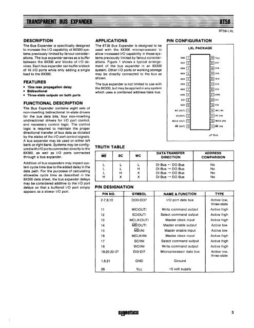
PIN CONFIGURATION<br />
I,XL PACKAGE<br />
Vcc<br />
016<br />
015<br />
014<br />
FUNCTIONAL DESCRIPTION<br />
The Bus Expander contains eight sets of<br />
non-inverting bidirectional tri-state drivers<br />
for the bus data bits, four non-inverting<br />
undirectional drivers for I/O port control,<br />
and necessary control logic. The control<br />
logic is required to maintain the proper<br />
directional transfer of bus data as dictated<br />
by the states of the I/O port control signals.<br />
A bus expander may be used on either left<br />
bank or right bank. Systems may be configured<br />
with I/O ports connected directly to the<br />
8X300, as well as I/O ports connected<br />
through a bus expander.<br />
Addition of bus expanders may impact system<br />
cycle time due to the added delay in the<br />
data path. For the purposes of calculating<br />
allowable cycle time as described in the<br />
8X300 data sheet, the bus expander delays<br />
may be considered additive to the I/O port<br />
delays so that a buffered I/O port simply<br />
appears as a slower I/O port.<br />
TRUTH TABLE<br />
ME SC WC<br />
MCLK (OUT)<br />
ME (OUT)<br />
DATA TRANSFER<br />
DIRECTION<br />
L L L 01 Bus - DO Bus<br />
L L H 01 Bus - DO Bus<br />
L H X 01 Bus - DO Bus<br />
H X X 01 Bus - DO Bus<br />
PIN DESIGNATION<br />
J.l.P Side<br />
ADDRESS<br />
COMPARISON<br />
PIN NO. SYMBOL NAME & FUNCTION TYPE<br />
2-7,9,10 000-007 I/O port data bus Active low,<br />
three-state<br />
11 WC(OUT) Write command output Active high<br />
12 SC(OUT) Select command output Active high<br />
13 MCLK(OUT) Master clock input Active high<br />
14 ME(OUT) Master enable output Active low<br />
-<br />
15 ME(lN) Master enable input Active low<br />
16 MCLK(IN) Master clock input Active high<br />
17 SC(lN) Select command output Active high<br />
18 WC(lN) Write command output Active high<br />
19,20,22-27 010-017 Microprocessor data bus Active low,<br />
three-state<br />
1,8,21 GND Ground<br />
No<br />
No<br />
No<br />
No<br />
28 Vee +5 volt supply<br />
!iI!lDOliC!i 3


