8x300 design guide - Al Kossow's Bitsavers - Trailing-Edge
8x300 design guide - Al Kossow's Bitsavers - Trailing-Edge
8x300 design guide - Al Kossow's Bitsavers - Trailing-Edge
You also want an ePaper? Increase the reach of your titles
YUMPU automatically turns print PDFs into web optimized ePapers that Google loves.
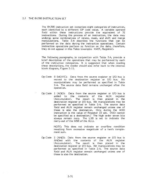
2.3 THE 8X300 INSTRUCTION SET<br />
The 8X300 instruction set comprises eight categories of instruction,<br />
each identified by a di fferent OP code value. A variable operand<br />
field within these instructions provide the equivalent of 32<br />
instructions. During the process of an instruction, the data may<br />
undergo some combinations of rotate, mask, and shift and merge<br />
manipulations. Table 2-4 describes the functions that can be<br />
performed on the data during the instruction operations. Certain<br />
instruction operations perform no function on the data, therefore,<br />
they do not appear in this Table (example: XMIT, Register).<br />
The following paragraphs, in conjunction with Table 2.4, provide a<br />
brief description of the operations that may be performed by each<br />
of the instruction categories. It is suggested that when reading<br />
these descriptions, the reader should also refer back to the internal<br />
block diagram, Figure 2-11.<br />
Op Code 0 (MO V E): Data from the source register or I/O bus is<br />
moved to the destination register or I/O bus. Bit<br />
manipulations may be performed as specified in Table<br />
2-4. The source data field remains unchanged after the<br />
operation.<br />
Op Code 1 (ADD): Data from the source register or I/O bus is<br />
added to the contents of the AUX register<br />
(Accumulator). The result is then placed in the<br />
destination register or I/O bus. Bit manipulations may be<br />
performed as specified in Table 2-4. The source data<br />
field and AUX register remain unchanged unless one of<br />
those is also the destination. Only during the ADD<br />
instruction is the value of Register 10 set. (RIO cannot<br />
be specified as a destination.) The high order seven bits<br />
always remain zero. The LSB is set to indicate the<br />
carry-out of the MSB of the ALU.<br />
NOTE: This does not indicate an overflow condition<br />
resulting from excessive magnitude of a two's complement<br />
sum.<br />
Op Code 2 (AND): Data from the source register or I/O bus is<br />
ANDed with the contents of the AUX register<br />
(Accumulator). The result is then placed in the<br />
destination register or I/O bus. Bit manipulations may be<br />
performed as specified in Table 2-4. The source data<br />
field and AUX register remain unchanged unless one of<br />
those is also the destination.<br />
2-31


