- Page 1 and 2:
THÈSE Pour obtenir le grade de DOC
- Page 3 and 4:
tel-00820068, version 1 - 3 May 201
- Page 5 and 6:
Remerciements tel-00820068, version
- Page 7 and 8:
Remerciements tel-00820068, version
- Page 9 and 10:
tel-00820068, version 1 - 3 May 201
- Page 11 and 12:
Sommaire tel-00820068, version 1 -
- Page 13 and 14:
Sommaire tel-00820068, version 1 -
- Page 15 and 16:
INTRODUCTION GENERALE tel-00820068,
- Page 17 and 18:
Introduction Générale chaque rég
- Page 19 and 20:
- CHAPITRE I - tel-00820068, versio
- Page 21 and 22:
Chapitre I: Le transistor MOSFET: f
- Page 23 and 24:
|Qsc| (C/m²) Chapitre I: Le transi
- Page 25 and 26:
Chapitre I: Le transistor MOSFET: f
- Page 27 and 28:
Chapitre I: Le transistor MOSFET: f
- Page 29 and 30:
Chapitre I: Le transistor MOSFET: f
- Page 31 and 32:
Chapitre I: Le transistor MOSFET: f
- Page 33 and 34:
Chapitre I: Le transistor MOSFET: f
- Page 35 and 36: Chapitre I: Le transistor MOSFET: f
- Page 37 and 38: Chapitre I: Le transistor MOSFET: f
- Page 39 and 40: Id (A) Pente sous le seuil S (mV/de
- Page 41 and 42: Oxyde de grille Chapitre I: Le tran
- Page 43 and 44: Délai (ps) xxx Chapitre I: Le tran
- Page 45 and 46: Nch moyen (cm -3 ) Vtlin (mV) Chapi
- Page 47 and 48: Travail de sortie (eV) Chapitre I:
- Page 49 and 50: Chapitre I: Le transistor MOSFET: f
- Page 51 and 52: Chapitre I: Le transistor MOSFET: f
- Page 53 and 54: Chapitre I: Le transistor MOSFET: f
- Page 55 and 56: Chapitre I: Le transistor MOSFET: f
- Page 57 and 58: Chapitre I: Le transistor MOSFET: f
- Page 59 and 60: I on (µA) Chapitre I: Le transisto
- Page 61 and 62: Chapitre I: Le transistor MOSFET: f
- Page 63 and 64: - CHAPITRE II - tel-00820068, versi
- Page 65 and 66: Chapitre II: Modélisation analytiq
- Page 67 and 68: Chapitre II: Modélisation analytiq
- Page 69 and 70: Vtlin (mV) Vtlin (mV) Vtlin (mV) Vt
- Page 71 and 72: Chapitre II: Modélisation analytiq
- Page 73 and 74: Vtlin (mV) Vtlin (mV) Vtlin (mV) Vt
- Page 75 and 76: SSlin (mV/dec) SSlin (mV/dec) SSsat
- Page 77 and 78: DIBL (mV) DIBL (mV) Vtlin (mV) Vtli
- Page 79 and 80: Cgc (F/µm²) Qi (C/µm²) Q inv (C
- Page 81 and 82: Chapitre II: Modélisation analytiq
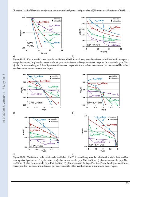
- Page 83 and 84: Chapitre II: Modélisation analytiq
- Page 85: Chapitre II: Modélisation analytiq
- Page 89 and 90: SCE(mV) DIBL(mV) SCE (mV) DIBL (mV)
- Page 91 and 92: Chapitre II: Modélisation analytiq
- Page 93 and 94: DIBL (mV) DIBL (mV) DIBL (mV) DIBL
- Page 95 and 96: SS (mV/dec) SS (mV/dec) Chapitre II
- Page 97 and 98: Vt (mV) Chapitre II: Modélisation
- Page 99 and 100: Chapitre II: Modélisation analytiq
- Page 101 and 102: Vtlin (mV) DIBL (mV) Vtlin (mV) DIB
- Page 103 and 104: Chapitre II: Modélisation analytiq
- Page 105 and 106: Chapitre II: Modélisation analytiq
- Page 107 and 108: Vgteff (V) Vgteff (V) Chapitre II:
- Page 109 and 110: Vdseff Vdseff (V) Ids (A) Chapitre
- Page 111 and 112: gm (A/V) gm (A/V) Id (A) Id (A) Id
- Page 113 and 114: Id (µA/µm) Id (µA/µm) gm (A/V.
- Page 115 and 116: Chapitre II: Modélisation analytiq
- Page 117 and 118: - CHAPITRE III - tel-00820068, vers
- Page 119 and 120: Chapitre III: Evaluation analytique
- Page 121 and 122: Chapitre III: Evaluation analytique
- Page 123 and 124: Chapitre III: Evaluation analytique
- Page 125 and 126: Chapitre III: Evaluation analytique
- Page 127 and 128: Chapitre III: Evaluation analytique
- Page 129 and 130: Cof (fF/µm) Cof(fF/µm) Cov (fF/µ
- Page 131 and 132: C (fF/µm) Chapitre III: Evaluation
- Page 133 and 134: C (fF/µm) C(fF/µm) Chapitre III:
- Page 135 and 136: Chapitre III: Evaluation analytique
- Page 137 and 138:
Ctot (fF/µm) Chapitre III: Evaluat
- Page 139 and 140:
Chapitre III: Evaluation analytique
- Page 141 and 142:
Chapitre III: Evaluation analytique
- Page 143 and 144:
Chapitre III: Evaluation analytique
- Page 145 and 146:
Chapitre III: Evaluation analytique
- Page 147 and 148:
C (fF) C (fF) Chapitre III: Evaluat
- Page 149 and 150:
Capa (fF/µm) Capa (fF/µm) Chapitr
- Page 151 and 152:
Chapitre III: Evaluation analytique
- Page 153 and 154:
Chapitre III: Evaluation analytique
- Page 155 and 156:
- CHAPITRE IV - tel-00820068, versi
- Page 157 and 158:
Vout (V) Chapitre IV: Application d
- Page 159 and 160:
Chapitre IV: Application des modèl
- Page 161 and 162:
Ids (mA/µm) R (Ohm.m) Ids (mA/µm)
- Page 163 and 164:
Ids (mA/µm) Chapitre IV: Applicati
- Page 165 and 166:
Delay (ps) Chapitre IV: Application
- Page 167 and 168:
Chapitre IV: Application des modèl
- Page 169 and 170:
Miniaturisation: More Moore Chapitr
- Page 171 and 172:
Chapitre IV: Application des modèl
- Page 173 and 174:
Chapitre IV: Application des modèl
- Page 175 and 176:
C wiring (fF) C (fF) Chapitre IV: A
- Page 177 and 178:
Delta Vt(mV) Chapitre IV: Applicati
- Page 179 and 180:
Chapitre IV: Application des modèl
- Page 181 and 182:
- CHAPITRE V - tel-00820068, versio
- Page 183 and 184:
Chapitre V: Evaluation des performa
- Page 185 and 186:
C (fF) C(fF) C (fF) Chapitre V: Eva
- Page 187 and 188:
Chapitre V: Evaluation des performa
- Page 189 and 190:
Chapitre V: Evaluation des performa
- Page 191 and 192:
Freq (Hz) Pdyn (W)) Chapitre V: Eva
- Page 193 and 194:
Id (A/µm) Id (A/µm) Chapitre V: E
- Page 195 and 196:
Chapitre V: Evaluation des performa
- Page 197 and 198:
Chapitre V: Evaluation des performa
- Page 199 and 200:
Id (A/µm) Id (A/µm) Chapitre V: E
- Page 201 and 202:
Chapitre V: Evaluation des performa
- Page 203 and 204:
Cinv + Cgd (fF/µm) Chapitre V: Eva
- Page 205 and 206:
Freq (Hz) Freq (Hz) Freq (Hz) Freq
- Page 207 and 208:
Pdyn (W) Pdyn (W) Chapitre V: Evalu
- Page 209 and 210:
Freq (Hz) Freq (Hz) Freq (Hz) Freq
- Page 211 and 212:
Freq (Hz) Freq (Hz) Pdyn (W) Pdyn (
- Page 213 and 214:
Charge en sortie de l'inverseur FO3
- Page 215 and 216:
Freq (Hz) Istat (A) Chapitre V: Eva
- Page 217 and 218:
Chapitre V: Evaluation des performa
- Page 219 and 220:
- CHAPITRE VI - tel-00820068, versi
- Page 221 and 222:
Chapitre VI: Comparaison des perfor
- Page 223 and 224:
Capacité grille totale (fF/µm) Ch
- Page 225 and 226:
Fréquence (Hz) Fréquence (Hz) Fr
- Page 227 and 228:
Istat (A) Charge en sortie de l'inv
- Page 229 and 230:
Chapitre VI: Comparaison des perfor
- Page 231 and 232:
Chapitre VI: Comparaison des perfor
- Page 233 and 234:
150 173 195 218 240 263 285 308 330
- Page 235 and 236:
Chapitre VI: Comparaison des perfor
- Page 237 and 238:
Chapitre VI: Comparaison des perfor
- Page 239 and 240:
CONCLUSION GENERALE tel-00820068, v
- Page 241 and 242:
Conclusion générale l’espaceur.
- Page 243 and 244:
Conclusion générale tel-00820068,
- Page 245 and 246:
BIBLIOGRAPHIE tel-00820068, version
- Page 247 and 248:
Bibliographie [Bidal 09] G. Bidal,
- Page 249 and 250:
Bibliographie [ELDO] [ELDO UDM manu
- Page 251 and 252:
Bibliographie [Hänsch 89] W. Häns
- Page 253 and 254:
Bibliographie [Mathieu 04] H. Mathi
- Page 255 and 256:
Bibliographie [Rafhay 10] [Ramey 03
- Page 257 and 258:
Bibliographie Understanding”. In
- Page 259 and 260:
PUBLICATIONS DE L’AUTEUR Articles
- Page 261 and 262:
Annexe: Utilisation de MASTAR VA 1.
- Page 263 and 264:
Annexe Définition du sous circuit
- Page 265 and 266:
Annexe 5.b. Structure du modèle Le
- Page 267 and 268:
tel-00820068, version 1 - 3 May 201
- Page 269 and 270:
tel-00820068, version 1 - 3 May 201