Solar Energy Perspectives - IEA
Solar Energy Perspectives - IEA
Solar Energy Perspectives - IEA

Create successful ePaper yourself
Turn your PDF publications into a flip-book with our unique Google optimized e-Paper software.
Chapter 6: <strong>Solar</strong> photovoltaics<br />
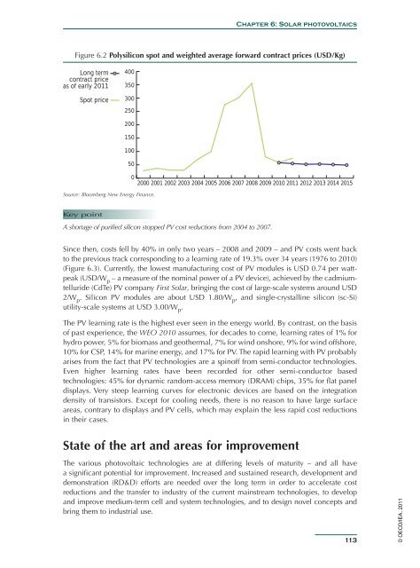
Figure 6.2 Polysilicon spot and weighted average forward contract prices (USD/Kg)<br />
Long term<br />
contract price<br />
as of early 2011<br />
Spot price<br />
400<br />
350<br />
300<br />
250<br />
200<br />
150<br />
100<br />
50<br />
0<br />
2000 2001 2002 2003 2004 2005 2006 2007 2008 2009 2010 2011 2012 2013 2014 2015<br />
Source: Bloomberg New <strong>Energy</strong> Finance.<br />
Key point<br />
Figure 6.2<br />
A shortage of purified silicon stopped PV cost reductions from 2004 to 2007.<br />
Since then, costs fell by 40% in only two years – 2008 and 2009 – and PV costs went back<br />
to the previous track corresponding to a learning rate of 19.3% over 34 years (1976 to 2010)<br />
(Figure 6.3). Currently, the lowest manufacturing cost of PV modules is USD 0.74 per wattpeak<br />
(USD/W p – a measure of the nominal power of a PV device), achieved by the cadmiumtelluride<br />
(CdTe) PV company First <strong>Solar</strong>, bringing the cost of large-scale systems around USD<br />
2/W p . Silicon PV modules are about USD 1.80/W p , and single-crystalline silicon (sc-Si)<br />
utility-scale systems at USD 3.00/W p .<br />
The PV learning rate is the highest ever seen in the energy world. By contrast, on the basis<br />
of past experience, the WEO 2010 assumes, for decades to come, learning rates of 1% for<br />
hydro power, 5% for biomass and geothermal, 7% for wind onshore, 9% for wind offshore,<br />
10% for CSP, 14% for marine energy, and 17% for PV. The rapid learning with PV probably<br />
arises from the fact that PV technologies are a spinoff from semi-conductor technologies.<br />
Even higher learning rates have been recorded for other semi-conductor based<br />
technologies: 45% for dynamic random-access memory (DRAM) chips, 35% for flat panel<br />
displays. Very steep learning curves for electronic devices are based on the integration<br />
density of transistors. Except for cooling needs, there is no reason to have large surface<br />
areas, contrary to displays and PV cells, which may explain the less rapid cost reductions<br />
in their cases.<br />
State of the art and areas for improvement<br />
The various photovoltaic technologies are at differing levels of maturity – and all have<br />
a significant potential for improvement. Increased and sustained research, development and<br />
demonstration (RD&D) efforts are needed over the long term in order to accelerate cost<br />
reductions and the transfer to industry of the current mainstream technologies, to develop<br />
and improve medium-term cell and system technologies, and to design novel concepts and<br />
bring them to industrial use.<br />
113<br />
© OECD/<strong>IEA</strong>, 2011