- Page 2 and 3:
Radio Frequency Integrated Circuit
- Page 4 and 5:
Radio Frequency Integrated Circuit
- Page 6 and 7:
Contents Foreword xv Acknowledgment
- Page 8 and 9:
Contents 3.8 Base Shot Noise Discus
- Page 10 and 11:
Contents 5.25 Packaging 135 5.25.1
- Page 12 and 13:
Contents 7.12 General Design Commen
- Page 14 and 15:
Contents 9.5 Some Simple Image Reje
- Page 16 and 17:
Foreword I enjoyed reading this boo
- Page 18:
Foreword estimates of parasitic cap
- Page 21 and 22:
xx Radio Frequency Integrated Circu
- Page 23 and 24:
2 Radio Frequency Integrated Circui
- Page 25 and 26:
4 Radio Frequency Integrated Circui
- Page 27 and 28:
6 Radio Frequency Integrated Circui
- Page 30 and 31:
2 Issues in RFIC Design, Noise, Lin
- Page 32 and 33:
Issues in RFIC Design, Noise, Linea
- Page 34 and 35:
Issues in RFIC Design, Noise, Linea
- Page 36 and 37:
Issues in RFIC Design, Noise, Linea
- Page 38 and 39:
The input noise is Issues in RFIC D
- Page 40 and 41:
Issues in RFIC Design, Noise, Linea
- Page 42 and 43:
Issues in RFIC Design, Noise, Linea
- Page 44 and 45:
Issues in RFIC Design, Noise, Linea
- Page 46 and 47:
Issues in RFIC Design, Noise, Linea
- Page 48 and 49:
Issues in RFIC Design, Noise, Linea
- Page 50 and 51:
Issues in RFIC Design, Noise, Linea
- Page 52 and 53:
Issues in RFIC Design, Noise, Linea
- Page 54 and 55:
Issues in RFIC Design, Noise, Linea
- Page 56 and 57:
Issues in RFIC Design, Noise, Linea
- Page 58 and 59:
2.5 Filtering Issues Issues in RFIC
- Page 60 and 61:
Issues in RFIC Design, Noise, Linea
- Page 62 and 63:
Issues in RFIC Design, Noise, Linea
- Page 64 and 65:
3 A Brief Review of Technology 3.1
- Page 66 and 67:
A Brief Review of Technology IC = I
- Page 68 and 69:
3.4 Small-Signal Model A Brief Revi
- Page 70 and 71:
3.6 High-Frequency Effects A Brief
- Page 72 and 73:
A Brief Review of Technology If thi
- Page 74 and 75:
A Brief Review of Technology Soluti
- Page 76 and 77:
A Brief Review of Technology 3.8 Ba
- Page 78 and 79:
A Brief Review of Technology • Pi
- Page 80 and 81:
A Brief Review of Technology 3.16,
- Page 82 and 83:
A Brief Review of Technology The tr
- Page 84 and 85:
4 Impedance Matching 4.1 Introducti
- Page 86 and 87:
Impedance Matching Z 2 = Z in + j
- Page 88 and 89:
Figure 4.5 A Smith chart. Impedance
- Page 90 and 91:
4.3 Impedance Matching Impedance Ma
- Page 92 and 93:
Impedance Matching Figure 4.9 Which
- Page 94 and 95:
Impedance Matching Figure 4.11 Lowp
- Page 96 and 97:
Impedance Matching section, convers
- Page 98 and 99:
Impedance Matching Much as in the p
- Page 100 and 101:
Impedance Matching Note that dots i
- Page 102 and 103: Impedance Matching Thus, in the fir
- Page 104 and 105: Impedance Matching The exact resist
- Page 106 and 107: Impedance Matching 4.10 Quality Fac
- Page 108 and 109: Impedance Matching Example 4.7 Matc
- Page 110 and 111: Impedance Matching line to change w
- Page 112 and 113: Impedance Matching S22 = b 2 a2 | a
- Page 114: Impedance Matching without the need
- Page 117 and 118: 96 Radio Frequency Integrated Circu
- Page 119 and 120: 98 Radio Frequency Integrated Circu
- Page 121 and 122: 100 Radio Frequency Integrated Circ
- Page 123 and 124: 102 Radio Frequency Integrated Circ
- Page 125 and 126: 104 Radio Frequency Integrated Circ
- Page 127 and 128: 106 Radio Frequency Integrated Circ
- Page 129 and 130: 108 Radio Frequency Integrated Circ
- Page 131 and 132: 110 Radio Frequency Integrated Circ
- Page 133 and 134: 112 Radio Frequency Integrated Circ
- Page 135 and 136: 114 Radio Frequency Integrated Circ
- Page 137 and 138: 116 Radio Frequency Integrated Circ
- Page 139 and 140: 118 Radio Frequency Integrated Circ
- Page 141 and 142: 120 Radio Frequency Integrated Circ
- Page 143 and 144: 122 Radio Frequency Integrated Circ
- Page 145 and 146: 124 Radio Frequency Integrated Circ
- Page 147 and 148: 126 Radio Frequency Integrated Circ
- Page 149 and 150: 128 Radio Frequency Integrated Circ
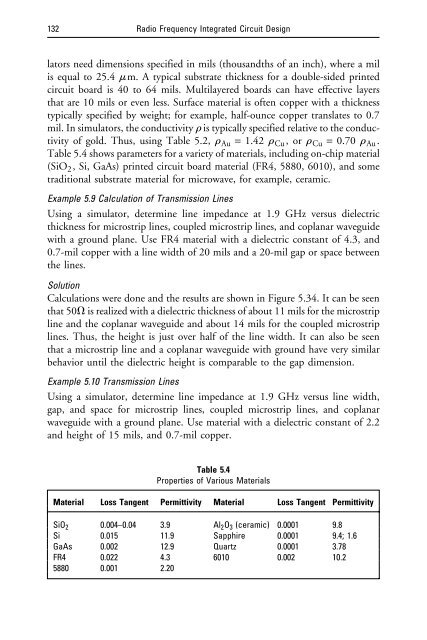
- Page 151: 130 Radio Frequency Integrated Circ
- Page 155 and 156: 134 Radio Frequency Integrated Circ
- Page 157 and 158: 136 Radio Frequency Integrated Circ
- Page 159 and 160: 138 Radio Frequency Integrated Circ
- Page 161 and 162: 140 Radio Frequency Integrated Circ
- Page 163 and 164: 142 Radio Frequency Integrated Circ
- Page 165 and 166: 144 Radio Frequency Integrated Circ
- Page 167 and 168: 146 Radio Frequency Integrated Circ
- Page 169 and 170: 148 Radio Frequency Integrated Circ
- Page 171 and 172: 150 Radio Frequency Integrated Circ
- Page 173 and 174: 152 Radio Frequency Integrated Circ
- Page 175 and 176: 154 Radio Frequency Integrated Circ
- Page 177 and 178: 156 Radio Frequency Integrated Circ
- Page 179 and 180: 158 Radio Frequency Integrated Circ
- Page 181 and 182: 160 Radio Frequency Integrated Circ
- Page 183 and 184: 162 Radio Frequency Integrated Circ
- Page 185 and 186: 164 Radio Frequency Integrated Circ
- Page 187 and 188: 166 Radio Frequency Integrated Circ
- Page 189 and 190: 168 Radio Frequency Integrated Circ
- Page 191 and 192: 170 Radio Frequency Integrated Circ
- Page 193 and 194: 172 Radio Frequency Integrated Circ
- Page 195 and 196: 174 Radio Frequency Integrated Circ
- Page 197 and 198: 176 Radio Frequency Integrated Circ
- Page 199 and 200: 178 Radio Frequency Integrated Circ
- Page 201 and 202: 180 Radio Frequency Integrated Circ
- Page 203 and 204:
182 Radio Frequency Integrated Circ
- Page 205 and 206:
184 Radio Frequency Integrated Circ
- Page 207 and 208:
186 Radio Frequency Integrated Circ
- Page 209 and 210:
188 Radio Frequency Integrated Circ
- Page 211 and 212:
190 Radio Frequency Integrated Circ
- Page 213 and 214:
192 Radio Frequency Integrated Circ
- Page 215 and 216:
194 Radio Frequency Integrated Circ
- Page 217 and 218:
196 Radio Frequency Integrated Circ
- Page 219 and 220:
198 Radio Frequency Integrated Circ
- Page 221 and 222:
200 Radio Frequency Integrated Circ
- Page 223 and 224:
202 Radio Frequency Integrated Circ
- Page 225 and 226:
204 Radio Frequency Integrated Circ
- Page 227 and 228:
206 Radio Frequency Integrated Circ
- Page 229 and 230:
208 Radio Frequency Integrated Circ
- Page 231 and 232:
210 Radio Frequency Integrated Circ
- Page 233 and 234:
212 Radio Frequency Integrated Circ
- Page 235 and 236:
214 Radio Frequency Integrated Circ
- Page 237 and 238:
216 Radio Frequency Integrated Circ
- Page 239 and 240:
218 Radio Frequency Integrated Circ
- Page 241 and 242:
220 Radio Frequency Integrated Circ
- Page 243 and 244:
222 Radio Frequency Integrated Circ
- Page 245 and 246:
224 Radio Frequency Integrated Circ
- Page 247 and 248:
226 Radio Frequency Integrated Circ
- Page 249 and 250:
228 Radio Frequency Integrated Circ
- Page 251 and 252:
230 Radio Frequency Integrated Circ
- Page 253 and 254:
232 Radio Frequency Integrated Circ
- Page 255 and 256:
234 Radio Frequency Integrated Circ
- Page 257 and 258:
236 Radio Frequency Integrated Circ
- Page 259 and 260:
238 Radio Frequency Integrated Circ
- Page 261 and 262:
240 Radio Frequency Integrated Circ
- Page 263 and 264:
242 Radio Frequency Integrated Circ
- Page 265 and 266:
244 Radio Frequency Integrated Circ
- Page 267 and 268:
246 Radio Frequency Integrated Circ
- Page 269 and 270:
248 Radio Frequency Integrated Circ
- Page 271 and 272:
250 Radio Frequency Integrated Circ
- Page 273 and 274:
252 Radio Frequency Integrated Circ
- Page 275 and 276:
254 Radio Frequency Integrated Circ
- Page 277 and 278:
256 Radio Frequency Integrated Circ
- Page 279 and 280:
258 Radio Frequency Integrated Circ
- Page 281 and 282:
260 Radio Frequency Integrated Circ
- Page 283 and 284:
262 Radio Frequency Integrated Circ
- Page 285 and 286:
264 Radio Frequency Integrated Circ
- Page 287 and 288:
266 Radio Frequency Integrated Circ
- Page 289 and 290:
268 Radio Frequency Integrated Circ
- Page 291 and 292:
270 Radio Frequency Integrated Circ
- Page 293 and 294:
272 Radio Frequency Integrated Circ
- Page 295 and 296:
274 Radio Frequency Integrated Circ
- Page 297 and 298:
276 Radio Frequency Integrated Circ
- Page 299 and 300:
278 Radio Frequency Integrated Circ
- Page 301 and 302:
280 Radio Frequency Integrated Circ
- Page 303 and 304:
282 Radio Frequency Integrated Circ
- Page 305 and 306:
284 Radio Frequency Integrated Circ
- Page 307 and 308:
286 Radio Frequency Integrated Circ
- Page 309 and 310:
288 Radio Frequency Integrated Circ
- Page 311 and 312:
290 Radio Frequency Integrated Circ
- Page 313 and 314:
292 Radio Frequency Integrated Circ
- Page 315 and 316:
294 Radio Frequency Integrated Circ
- Page 317 and 318:
296 Radio Frequency Integrated Circ
- Page 319 and 320:
298 Radio Frequency Integrated Circ
- Page 321 and 322:
300 Radio Frequency Integrated Circ
- Page 323:
302 Radio Frequency Integrated Circ
- Page 326 and 327:
Voltage-Controlled Oscillators back
- Page 328 and 329:
I C_AVE = 1 Voltage-Controlled Osci
- Page 330 and 331:
Voltage-Controlled Oscillators Loop
- Page 332 and 333:
Voltage-Controlled Oscillators freq
- Page 334 and 335:
Voltage-Controlled Oscillators Figu
- Page 336 and 337:
Voltage-Controlled Oscillators from
- Page 338:
Voltage-Controlled Oscillators [10]
- Page 341 and 342:
320 Radio Frequency Integrated Circ
- Page 343 and 344:
322 Radio Frequency Integrated Circ
- Page 345 and 346:
324 Radio Frequency Integrated Circ
- Page 347 and 348:
326 Radio Frequency Integrated Circ
- Page 349 and 350:
328 Radio Frequency Integrated Circ
- Page 351 and 352:
330 Radio Frequency Integrated Circ
- Page 353 and 354:
332 Radio Frequency Integrated Circ
- Page 355 and 356:
334 Radio Frequency Integrated Circ
- Page 357 and 358:
336 Radio Frequency Integrated Circ
- Page 359 and 360:
338 Radio Frequency Integrated Circ
- Page 361 and 362:
340 Radio Frequency Integrated Circ
- Page 363 and 364:
342 Radio Frequency Integrated Circ
- Page 365 and 366:
344 Radio Frequency Integrated Circ
- Page 367 and 368:
346 Radio Frequency Integrated Circ
- Page 370 and 371:
10 Power Amplifiers 10.1 Introducti
- Page 372 and 373:
Power Amplifiers where G is the pow
- Page 374 and 375:
Power Amplifiers Figure 10.4 Optima
- Page 376 and 377:
Power Amplifiers Figure 10.8 Power
- Page 378 and 379:
Power Amplifiers Figure 10.9 Curren
- Page 380 and 381:
Power Amplifiers The efficiency is
- Page 382 and 383:
Power Amplifiers sinusoid), this pe
- Page 384 and 385:
Power Amplifiers Note that this agr
- Page 386 and 387:
Power Amplifiers stabilization. The
- Page 388 and 389:
Power Amplifiers Solution The first
- Page 390 and 391:
Power Amplifiers Figure 10.22 Class
- Page 392 and 393:
Figure 10.24 Class E waveforms. Pow
- Page 394 and 395:
Power Amplifiers B = 0.1836 0.81Q R
- Page 396 and 397:
Power Amplifiers Figure 10.25 Initi
- Page 398 and 399:
Power Amplifiers added to the funda
- Page 400 and 401:
Power Amplifiers 10.8.1 Variation o
- Page 402 and 403:
Example 10.4 Class F Power Amplifie
- Page 404 and 405:
Figure 10.36 Class H amplifier. Pow
- Page 406 and 407:
Power Amplifiers ered quite good. O
- Page 408 and 409:
Power Amplifiers Figure 10.39 Time-
- Page 410 and 411:
Figure 10.42 High-Q matching circui
- Page 412 and 413:
Figure 10.44 Multiple transistors.
- Page 414 and 415:
Power Amplifiers Figure 10.48 Combi
- Page 416 and 417:
Power Amplifiers have very narrow b
- Page 418 and 419:
Power Amplifiers Figure 10.53 Feedf
- Page 420 and 421:
Power Amplifiers in class A (input
- Page 422 and 423:
About the Authors John Rogers recei
- Page 424 and 425:
Index 1-dB compression point, 30-32
- Page 426 and 427:
Index Damped resonator, 247-48 Emit
- Page 428 and 429:
Index Local oscillator, 5 Mixing co
- Page 430 and 431:
Index Quadrature phase shift keying