- Page 1 and 2:
REFERENCE MANUAL Copernicus GPS Re
- Page 3 and 4:
Corporate Office Trimble Navigation
- Page 6 and 7:
Table of Contents Table of Contents
- Page 8 and 9:
Table of Contents 7 MECHANICAL SPEC
- Page 10 and 11:
Table of Contents Command Packet 0x
- Page 12 and 13:
Table of Contents X1 Extended Statu
- Page 14 and 15:
CHAPTER 1 STARTER KIT 1 In this cha
- Page 16 and 17:
STARTER KIT 1 Starter Kit The Coper
- Page 18 and 19:
STARTER KIT 1 Figure 1.3 USB Cable
- Page 20 and 21:
STARTER KIT 1 Interface Connections
- Page 22 and 23:
STARTER KIT 1 Removing the Referenc
- Page 24 and 25:
STARTER KIT 1 Quick Start Guide 1.
- Page 26 and 27:
STARTER KIT 1 Trimble GPS Monitor T
- Page 28 and 29:
STARTER KIT 1 4. Click the Device M
- Page 30 and 31:
STARTER KIT 1 Connect to the GPS Re
- Page 32 and 33: STARTER KIT 1 Configure GPS Ports 1
- Page 34 and 35: STARTER KIT 1 Configure PPS Output
- Page 36 and 37: STARTER KIT 1 Creating a Log Follow
- Page 38 and 39: STARTER KIT 1 3. Select one of the
- Page 40 and 41: CHAPTER 2 PRODUCT DESCRIPTION 2 In
- Page 42 and 43: PRODUCT DESCRIPTION 2 Block Diagram
- Page 44 and 45: PRODUCT DESCRIPTION 2 Electrical El
- Page 46 and 47: PRODUCT DESCRIPTION 2 Absolute Mini
- Page 48 and 49: PRODUCT DESCRIPTION 2 Power Consump
- Page 50 and 51: CHAPTER 3 INTERFACE CHARACTERISTICS
- Page 52 and 53: INTERFACE CHARACTERISTICS 3 Pin Des
- Page 54 and 55: INTERFACE CHARACTERISTICS 3 Table 3
- Page 56 and 57: INTERFACE CHARACTERISTICS 3 Serial
- Page 58 and 59: INTERFACE CHARACTERISTICS 3 Acquiri
- Page 60 and 61: INTERFACE CHARACTERISTICS 3 Enablin
- Page 62 and 63: CHAPTER 4 OPERATING MODES 4 In this
- Page 64 and 65: OPERATING MODES 4 Changing the Run/
- Page 66 and 67: OPERATING MODES 4 Serial Port Activ
- Page 68 and 69: OPERATING MODES 4 Saving Almanac, E
- Page 70 and 71: CHAPTER 5 APPLICATION CIRCUITS 5 In
- Page 72 and 73: APPLICATION CIRCUITS 5 Figure 5.2 P
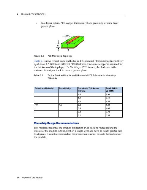
- Page 74 and 75: APPLICATION CIRCUITS 5 • Antenna
- Page 76 and 77: APPLICATION CIRCUITS 5 Following is
- Page 78 and 79: CHAPTER 6 RF LAYOUT CONSIDERATIONS
- Page 80 and 81: RF LAYOUT CONSIDERATIONS 6 In the p
- Page 84 and 85: RF LAYOUT CONSIDERATIONS 6 Striplin
- Page 86 and 87: CHAPTER 7 MECHANICAL SPECIFICATIONS
- Page 88 and 89: MECHANICAL SPECIFICATIONS 7 Solderi
- Page 90 and 91: MECHANICAL SPECIFICATIONS 7 Paste M
- Page 92 and 93: CHAPTER 8 PACKAGING 8 In this chapt
- Page 94 and 95: PACKAGING 8 Reel The 13-inch reel t
- Page 96 and 97: CHAPTER 9 SHIPPING and HANDLING 9 I
- Page 98 and 99: SHIPPING and HANDLING 9 Moisture Pr
- Page 100 and 101: SHIPPING and HANDLING 9 Recommended
- Page 102 and 103: SHIPPING and HANDLING 9 Grounding t
- Page 104 and 105: CHAPTER 10 COPERNICUS REFERENCE BOA
- Page 106 and 107: COPERNICUS REFERENCE BOARD 10 IMAGE
- Page 108 and 109: COPERNICUS REFERENCE BOARD 10 Refer
- Page 110 and 111: COPERNICUS REFERENCE BOARD 10 Refer
- Page 112 and 113: COPERNICUS REFERENCE BOARD 10 Refer
- Page 114 and 115: CHAPTER 11 FIRMWARE UPGRADE 11 In t
- Page 116 and 117: FIRMWARE UPGRADE 11 Firmware Binary
- Page 118 and 119: FIRMWARE UPGRADE 11 Pseudo-Code Exp
- Page 120 and 121: FIRMWARE UPGRADE 11 Error Recovery
- Page 122 and 123: FIRMWARE UPGRADE 11 Packet ID - 0x8
- Page 124 and 125: FIRMWARE UPGRADE 11 Packet ID - 0x8
- Page 126 and 127: FIRMWARE UPGRADE 11 Loading Firmwar
- Page 128 and 129: APPENDIX A TRIMBLE STANDARD INTERFA
- Page 130 and 131: TRIMBLE STANDARD INTERFACE PROTOCOL
- Page 132 and 133:
TRIMBLE STANDARD INTERFACE PROTOCOL
- Page 134 and 135:
TRIMBLE STANDARD INTERFACE PROTOCOL
- Page 136 and 137:
TRIMBLE STANDARD INTERFACE PROTOCOL
- Page 138 and 139:
TRIMBLE STANDARD INTERFACE PROTOCOL
- Page 140 and 141:
TRIMBLE STANDARD INTERFACE PROTOCOL
- Page 142 and 143:
TRIMBLE STANDARD INTERFACE PROTOCOL
- Page 144 and 145:
TRIMBLE STANDARD INTERFACE PROTOCOL
- Page 146 and 147:
TRIMBLE STANDARD INTERFACE PROTOCOL
- Page 148 and 149:
TRIMBLE STANDARD INTERFACE PROTOCOL
- Page 150 and 151:
TRIMBLE STANDARD INTERFACE PROTOCOL
- Page 152 and 153:
TRIMBLE STANDARD INTERFACE PROTOCOL
- Page 154 and 155:
TRIMBLE STANDARD INTERFACE PROTOCOL
- Page 156 and 157:
TRIMBLE STANDARD INTERFACE PROTOCOL
- Page 158 and 159:
TRIMBLE STANDARD INTERFACE PROTOCOL
- Page 160 and 161:
TRIMBLE STANDARD INTERFACE PROTOCOL
- Page 162 and 163:
TRIMBLE STANDARD INTERFACE PROTOCOL
- Page 164 and 165:
TRIMBLE STANDARD INTERFACE PROTOCOL
- Page 166 and 167:
TRIMBLE STANDARD INTERFACE PROTOCOL
- Page 168 and 169:
TRIMBLE STANDARD INTERFACE PROTOCOL
- Page 170 and 171:
TRIMBLE STANDARD INTERFACE PROTOCOL
- Page 172 and 173:
TRIMBLE STANDARD INTERFACE PROTOCOL
- Page 174 and 175:
TRIMBLE STANDARD INTERFACE PROTOCOL
- Page 176 and 177:
TRIMBLE STANDARD INTERFACE PROTOCOL
- Page 178 and 179:
TRIMBLE STANDARD INTERFACE PROTOCOL
- Page 180 and 181:
TRIMBLE STANDARD INTERFACE PROTOCOL
- Page 182 and 183:
TRIMBLE STANDARD INTERFACE PROTOCOL
- Page 184 and 185:
TRIMBLE STANDARD INTERFACE PROTOCOL
- Page 186 and 187:
TRIMBLE STANDARD INTERFACE PROTOCOL
- Page 188 and 189:
TRIMBLE STANDARD INTERFACE PROTOCOL
- Page 190 and 191:
TRIMBLE STANDARD INTERFACE PROTOCOL
- Page 192 and 193:
TRIMBLE STANDARD INTERFACE PROTOCOL
- Page 194 and 195:
APPENDIX B TRIMBLE ASCII INTERFACE
- Page 196 and 197:
TRIMBLE ASCII INTERFACE PROTOCOL (T
- Page 198 and 199:
TRIMBLE ASCII INTERFACE PROTOCOL (T
- Page 200 and 201:
TRIMBLE ASCII INTERFACE PROTOCOL (T
- Page 202 and 203:
TRIMBLE ASCII INTERFACE PROTOCOL (T
- Page 204 and 205:
TRIMBLE ASCII INTERFACE PROTOCOL (T
- Page 206 and 207:
TRIMBLE ASCII INTERFACE PROTOCOL (T
- Page 208 and 209:
TRIMBLE ASCII INTERFACE PROTOCOL (T
- Page 210 and 211:
TRIMBLE ASCII INTERFACE PROTOCOL (T
- Page 212 and 213:
TRIMBLE ASCII INTERFACE PROTOCOL (T
- Page 214 and 215:
TRIMBLE ASCII INTERFACE PROTOCOL (T
- Page 216 and 217:
TRIMBLE ASCII INTERFACE PROTOCOL (T
- Page 218 and 219:
TRIMBLE ASCII INTERFACE PROTOCOL (T
- Page 220 and 221:
APPENDIX C NMEA 0183 C In this appe
- Page 222 and 223:
NMEA 0183 C The NMEA 0183 Communica
- Page 224 and 225:
NMEA 0183 C Note - Spaces are only
- Page 226 and 227:
NMEA 0183 C General NMEA Parser Req
- Page 228 and 229:
NMEA 0183 C Table C.4 Copernicus GP
- Page 230 and 231:
NMEA 0183 C GLL - Geographic Positi
- Page 232 and 233:
NMEA 0183 C RMC - Recommended Minim
- Page 234 and 235:
NMEA 0183 C AH - Almanac Health Thi
- Page 236 and 237:
NMEA 0183 C AS - Almanac Status Thi
- Page 238 and 239:
NMEA 0183 C EP - Ephemeris This sen
- Page 240 and 241:
NMEA 0183 C IO Ionosphere This sent
- Page 242 and 243:
NMEA 0183 C PS - PPS Configuration
- Page 244 and 245:
NMEA 0183 C RT - Reset This sentenc
- Page 246 and 247:
NMEA 0183 C Table C.29 SG - Set Bit
- Page 248 and 249:
NMEA 0183 C TF - Receiver Status an
- Page 250 and 251:
NMEA 0183 C VR - Version This sente