- Page 2 and 3:
Digital ElectronicsDigital Electron
- Page 4 and 5:
Copyright © 2007John Wiley & Sons
- Page 6 and 7:
ContentsPrefacexxi1 Number Systems
- Page 8 and 9:
ContentsixReview Questions 67Proble
- Page 10 and 11:
Contentsxi6.3.8 Theorem 8 1966.3.9
- Page 12 and 13:
Contentsxiii9.11.3 Verilog 3399.11.
- Page 14 and 15:
Contentsxv12.2.5 Nonlinearity and D
- Page 16 and 17:
Contentsxvii13.10.3 80286 Microproc
- Page 18 and 19:
ContentsxixReview Questions 650Prob
- Page 20 and 21:
PrefaceDigital electronics is essen
- Page 22 and 23:
Prefacexxiiilogic analysers, freque
- Page 25 and 26:
Number Systems 3The value or magnit
- Page 27 and 28:
Number Systems 5The 1’s complemen
- Page 29 and 30:
Number Systems 7• The fractional
- Page 31 and 32:
Number Systems 9• The octal equiv
- Page 33 and 34:
Number Systems 11Solution• The gi
- Page 35 and 36:
Number Systems 13Hexadecimal system
- Page 37 and 38:
Number Systems 15Byte-1 Byte-2 Byte
- Page 39 and 40:
Number Systems 17Therefore, the exp
- Page 41 and 42:
2Binary CodesThe present chapter is
- Page 43 and 44:
Binary Codes 212.1.3 Higher-Density
- Page 45 and 46:
Binary Codes 23Fractional part = .7
- Page 47 and 48:
Binary Codes 252.3.2 Gray Code-Bina
- Page 49 and 50: Binary Codes 27Solution(a) The bina
- Page 51 and 52: Binary Codes 29Table 2.6(continued)
- Page 53 and 54: Binary Codes 31Table 2.6(continued)
- Page 55 and 56: Binary Codes 33Table 2.7(continued)
- Page 57 and 58: Binary Codes 35Table 2.7(continued)
- Page 59 and 60: Binary Codes 37Table 2.7(continued)
- Page 61 and 62: Binary Codes 39fabDPegdc(a)afbegcDP
- Page 63 and 64: Binary Codes 412.6.1 Parity CodeA p
- Page 65 and 66: Binary Codes 43Table 2.9Generation
- Page 67 and 68: Binary Codes 456. What is a parity
- Page 69 and 70: 48 Digital ElectronicsTable 3.1Bina
- Page 71 and 72: 50 Digital ElectronicsCase 1• Con
- Page 73 and 74: 52 Digital Electronics2. (AF1.B3) 1
- Page 75 and 76: 54 Digital ElectronicsCase 2• Let
- Page 77 and 78: 56 Digital ElectronicsExample 3.4Su
- Page 79 and 80: 58 Digital Electronics0110 1000 rep
- Page 81 and 82: 60 Digital ElectronicsTable 3.3Mult
- Page 83 and 84: 62 Digital ElectronicsTable 3.6algo
- Page 85 and 86: 64 Digital ElectronicsTable 3.8 Exa
- Page 87 and 88: 66 Digital Electronicsquotient is g
- Page 89 and 90: 68 Digital Electronics5. Prove that
- Page 91 and 92: 70 Digital ElectronicsIf the two vo
- Page 93 and 94: 72 Digital ElectronicsABCY=A+B+C(a)
- Page 95 and 96: 74 Digital ElectronicsABY=A.B(a)A00
- Page 97 and 98: 76 Digital ElectronicsXY=X(a)XY=XX0
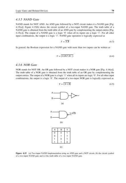
- Page 99: 78 Digital ElectronicsAY1BCY(a)ABCD
- Page 103 and 104: 82 Digital ElectronicsABCDY=A.B.C.D
- Page 105 and 106: 84 Digital Electronics'1''1'ab c d
- Page 107 and 108: 86 Digital ElectronicsAY=A(a)ABY=A+
- Page 109 and 110: 88 Digital ElectronicsAYBEA00001111
- Page 111 and 112: 90 Digital ElectronicsABCD(AB+CD+EF
- Page 113 and 114: 92 Digital Electronics(a)(b)4V (vol
- Page 115 and 116: 94 Digital Electronics'1'I/PI/P(Vol
- Page 117 and 118: 96 Digital ElectronicsIOHIIHIIHIIH(
- Page 119 and 120: 98 Digital ElectronicsThe output of
- Page 121 and 122: 100 Digital ElectronicsE1LLHE2LHXOp
- Page 123 and 124: 102 Digital Electronics1A1B2A2B3A3B
- Page 125 and 126: 104 Digital Electronics4.13.2 AND G
- Page 127 and 128: 106 Digital ElectronicsFigure 4.53(
- Page 129 and 130: 108 Digital ElectronicsTable 4.1(co
- Page 131 and 132: 110 Digital Electronics(c) a three-
- Page 133 and 134: 112 Digital ElectronicsFigure 4.59(
- Page 135 and 136: 114 Digital Electronics6. It is pro
- Page 137 and 138: 116 Digital Electronicsother and th
- Page 139 and 140: 118 Digital Electronics5.1.2.3 ECL
- Page 141 and 142: 120 Digital Electronics• LOW-leve
- Page 143 and 144: 122 Digital Electronics• Enable t
- Page 145 and 146: 124 Digital ElectronicsExample 5.2R
- Page 147 and 148: 126 Digital Electronics+VCC+VCCR 3I
- Page 149 and 150: 128 Digital Electronics4K 1301.6KVC
- Page 151 and 152:
130 Digital Electronicsbe in cut-of
- Page 153 and 154:
132 Digital ElectronicsVCC4K1.6KInp
- Page 155 and 156:
134 Digital Electronicslow-power TT
- Page 157 and 158:
136 Digital Electronics5.3.5.1 Char
- Page 159 and 160:
138 Digital ElectronicsVCCR 137KR 2
- Page 161 and 162:
140 Digital Electronicsfeatures of
- Page 163 and 164:
142 Digital ElectronicsFigure 5.24H
- Page 165 and 166:
144 Digital Electronics+VCC+VCCR1IO
- Page 167 and 168:
146 Digital ElectronicsFigure 5.30
- Page 169 and 170:
148 Digital Electronics5.4.1.2 MECL
- Page 171 and 172:
150 Digital ElectronicsFigure 5.33E
- Page 173 and 174:
152 Digital Electronicsfunctions as
- Page 175 and 176:
154 Digital ElectronicsVDDAQ1BQ 2Y=
- Page 177 and 178:
156 Digital ElectronicsVDDAQ 1BQ2Q5
- Page 179 and 180:
158 Digital ElectronicsFigure 5.42T
- Page 181 and 182:
160 Digital Electronics+VDDQ7Q8Q5Q6
- Page 183 and 184:
162 Digital ElectronicsFigure 5.46C
- Page 185 and 186:
164 Digital ElectronicsFigure 5.49(
- Page 187 and 188:
166 Digital Electronicslogic status
- Page 189 and 190:
168 Digital Electronics5.5.2.4 74AC
- Page 191 and 192:
170 Digital Electronics+VDDA+VDDA -
- Page 193 and 194:
172 Digital Electronics+VDDAQ 1Q 3Q
- Page 195 and 196:
174 Digital Electronicsthe conducti
- Page 197 and 198:
176 Digital Electronics+VRQ3Q4AAQ 2
- Page 199 and 200:
178 Digital Electronics74S00174S002
- Page 201 and 202:
180 Digital Electronicsvoltage of 5
- Page 203 and 204:
182 Digital Electronics+5V10KI/PTTL
- Page 205 and 206:
184 Digital ElectronicsI/PCMOSCMOS-
- Page 207 and 208:
186 Digital ElectronicsFigure 5.66
- Page 209 and 210:
6Boolean Algebra andSimplification
- Page 211 and 212:
Boolean Algebra and Simplification
- Page 213 and 214:
Boolean Algebra and Simplification
- Page 215 and 216:
Boolean Algebra and Simplification
- Page 217 and 218:
Boolean Algebra and Simplification
- Page 219 and 220:
Boolean Algebra and Simplification
- Page 221 and 222:
Boolean Algebra and Simplification
- Page 223 and 224:
Boolean Algebra and Simplification
- Page 225 and 226:
Boolean Algebra and Simplification
- Page 227 and 228:
Boolean Algebra and Simplification
- Page 229 and 230:
Boolean Algebra and Simplification
- Page 231 and 232:
Boolean Algebra and Simplification
- Page 233 and 234:
Boolean Algebra and Simplification
- Page 235 and 236:
Boolean Algebra and Simplification
- Page 237 and 238:
Boolean Algebra and Simplification
- Page 239 and 240:
Boolean Algebra and Simplification
- Page 241 and 242:
Boolean Algebra and Simplification
- Page 243 and 244:
Boolean Algebra and Simplification
- Page 245 and 246:
Boolean Algebra and Simplification
- Page 247 and 248:
Boolean Algebra and Simplification
- Page 249 and 250:
Boolean Algebra and Simplification
- Page 251 and 252:
Boolean Algebra and Simplification
- Page 253 and 254:
234 Digital Electronics'n'InputsCom
- Page 255 and 256:
236 Digital Electronicsof Boolean e
- Page 257 and 258:
238 Digital ElectronicsC in C out11
- Page 259 and 260:
240 Digital ElectronicsABC inABC in
- Page 261 and 262:
242 Digital ElectronicsABHalfSubtra
- Page 263 and 264:
244 Digital ElectronicsB inABDB o(a
- Page 265 and 266:
246 Digital ElectronicsFigure 7.19F
- Page 267 and 268:
248 Digital ElectronicsTable 7.1 Re
- Page 269 and 270:
250 Digital ElectronicsExample 7.1F
- Page 271 and 272:
252 Digital ElectronicsSolutionLet
- Page 273 and 274:
254 Digital ElectronicsB 7 B 6 B 5
- Page 275 and 276:
256 Digital Electronicsotherwise ha
- Page 277 and 278:
258 Digital ElectronicsFigure 7.32F
- Page 279 and 280:
260 Digital Electronics7.7 Arithmet
- Page 281 and 282:
262 Digital ElectronicsFigure 7.36F
- Page 283 and 284:
264 Digital ElectronicsTable 7.2 Fu
- Page 285 and 286:
266 Digital ElectronicsTable 7.3Com
- Page 287 and 288:
268 Digital ElectronicsFurther Read
- Page 289 and 290:
270 Digital ElectronicsI 0I 1I 2I 3
- Page 291 and 292:
272 Digital ElectronicsI 0I 12-to-1
- Page 293 and 294:
274 Digital ElectronicsI 0I 1YI 2I
- Page 295 and 296:
276 Digital ElectronicsTable 8.2 Im
- Page 297 and 298:
278 Digital ElectronicsSolution•
- Page 299 and 300:
280 Digital Electronics8.1.4 Cascad
- Page 301 and 302:
282 Digital ElectronicsD 0 D 1 D 2
- Page 303 and 304:
284 Digital ElectronicsExample 8.4W
- Page 305 and 306:
286 Digital ElectronicsAB2-to-40123
- Page 307 and 308:
288 Digital ElectronicsABC2 2012345
- Page 309 and 310:
290 Digital Electronics0CBA12 22F3-
- Page 311 and 312:
292 Digital Electronics(a) Since bo
- Page 313 and 314:
294 Digital ElectronicsTable 8.12(c
- Page 315 and 316:
296 Digital ElectronicsD 0I 0I 1S 0
- Page 317 and 318:
298 Digital ElectronicsFurther Read
- Page 319 and 320:
300 Digital Electronicslogic functi
- Page 321 and 322:
302 Digital Electronics3. In the ca
- Page 323 and 324:
304 Digital ElectronicsD C B AProgr
- Page 325 and 326:
306 Digital Electronicsa GAL device
- Page 327 and 328:
308 Digital Electronicslarge memory
- Page 329 and 330:
310 Digital ElectronicsA B C D EHar
- Page 331 and 332:
312 Digital ElectronicsSolution(a)
- Page 333 and 334:
314 Digital ElectronicsInputs(n)(k)
- Page 335 and 336:
316 Digital ElectronicsABCiSCoFigur
- Page 337 and 338:
318 Digital ElectronicsAA 1 0B1B000
- Page 339 and 340:
320 Digital ElectronicsA1A0B1B0O/P-
- Page 341 and 342:
322 Digital ElectronicsProgrammable
- Page 343 and 344:
324 Digital ElectronicsCDAB00 01 11
- Page 345 and 346:
326 Digital ElectronicsABCDP Q R SF
- Page 347 and 348:
328 Digital ElectronicsFigures 9.23
- Page 349 and 350:
330 Digital ElectronicsInputsGlobal
- Page 351 and 352:
332 Digital ElectronicsDQO/P4-input
- Page 353 and 354:
334 Digital Electronicsthat have ev
- Page 355 and 356:
336 Digital ElectronicsLogic CellSR
- Page 357 and 358:
338 Digital ElectronicsDesign Entry
- Page 359 and 360:
340 Digital Electronicsbraces to de
- Page 361 and 362:
342 Digital ElectronicsCLK120VccI02
- Page 363 and 364:
344 Digital ElectronicsCLK120VccI02
- Page 365 and 366:
346 Digital ElectronicsARDCLKQQ4to1
- Page 367 and 368:
348 Digital ElectronicsCentral Swit
- Page 369 and 370:
350 Digital ElectronicsTable 9.6Sal
- Page 371 and 372:
352 Digital ElectronicsQSA1A2A3A4A5
- Page 373 and 374:
354 Digital Electronics3. Determine
- Page 375 and 376:
10Flip-Flops and Related DevicesHav
- Page 377 and 378:
Flip-Flops and Related Devices 359V
- Page 379 and 380:
Flip-Flops and Related Devices 361+
- Page 381 and 382:
Flip-Flops and Related Devices 363p
- Page 383 and 384:
Flip-Flops and Related Devices 365+
- Page 385 and 386:
Flip-Flops and Related Devices 367+
- Page 387 and 388:
Flip-Flops and Related Devices 369v
- Page 389 and 390:
Flip-Flops and Related Devices 371V
- Page 391 and 392:
Flip-Flops and Related Devices 3731
- Page 393 and 394:
Flip-Flops and Related Devices 375S
- Page 395 and 396:
Flip-Flops and Related Devices 377S
- Page 397 and 398:
Flip-Flops and Related Devices 379t
- Page 399 and 400:
Flip-Flops and Related Devices 381S
- Page 401 and 402:
Flip-Flops and Related Devices 383C
- Page 403 and 404:
Flip-Flops and Related Devices 385J
- Page 405 and 406:
Flip-Flops and Related Devices 387P
- Page 407 and 408:
Flip-Flops and Related Devices 389a
- Page 409 and 410:
Flip-Flops and Related Devices 391F
- Page 411 and 412:
Flip-Flops and Related Devices 393Q
- Page 413 and 414:
Flip-Flops and Related Devices 395I
- Page 415 and 416:
Flip-Flops and Related Devices 397D
- Page 417 and 418:
Flip-Flops and Related Devices 3991
- Page 419 and 420:
Flip-Flops and Related Devices 401C
- Page 421 and 422:
Flip-Flops and Related Devices 403+
- Page 423 and 424:
Flip-Flops and Related Devices 405C
- Page 425 and 426:
Flip-Flops and Related Devices 407w
- Page 427 and 428:
Flip-Flops and Related Devices 409(
- Page 429 and 430:
11Counters and RegistersCounters an
- Page 431 and 432:
Counters and Registers 413ripple co
- Page 433 and 434:
Counters and Registers 415Table 11.
- Page 435 and 436:
Q 00Counters and Registers 4171JQ 0
- Page 437 and 438:
Counters and Registers 419Table 11.
- Page 439 and 440:
Counters and Registers 421'1'JPrQ A
- Page 441 and 442:
Counters and Registers 42311.5 Sync
- Page 443 and 444:
Counters and Registers 425Table 11.
- Page 445 and 446:
Counters and Registers 427Presettab
- Page 447 and 448:
Counters and Registers 429Clk(D)Q 0
- Page 449 and 450:
Counters and Registers 431Input AAO
- Page 451 and 452:
Counters and Registers 433ClockA-Ou
- Page 453 and 454:
Counters and Registers 435PLP3 P2 P
- Page 455 and 456:
Counters and Registers 437+V CCGNDU
- Page 457 and 458:
Counters and Registers 439Table 11.
- Page 459 and 460:
Counters and Registers 441The circu
- Page 461 and 462:
Counters and Registers 443Table 11.
- Page 463 and 464:
Counters and Registers 445CX (C) 1B
- Page 465 and 466:
Counters and Registers 447Figure 11
- Page 467 and 468:
Counters and Registers 449to the dr
- Page 469 and 470:
Counters and Registers 451Table 11.
- Page 471 and 472:
Counters and Registers 453Figure 11
- Page 473 and 474:
Counters and Registers 455Figure 11
- Page 475 and 476:
Figure 11.43 Logic diagram of IC 74
- Page 477 and 478:
Counters and Registers 45911.13 Shi
- Page 479 and 480:
Counters and Registers 461Clock-Inp
- Page 481 and 482:
Counters and Registers 4631JFClockC
- Page 483 and 484:
Counters and Registers 465R0(1)R0(2
- Page 485 and 486:
Counters and Registers 467(9)CLK C1
- Page 487 and 488:
Counters and Registers 469Table 11.
- Page 489 and 490:
Counters and Registers 4711OutputCJ
- Page 491 and 492:
12Data Conversion Circuits - D/Aand
- Page 493 and 494:
Data Conversion Circuits - D/A and
- Page 495 and 496:
Data Conversion Circuits - D/A and
- Page 497 and 498:
{Data Conversion Circuits - D/A and
- Page 499 and 500:
Data Conversion Circuits - D/A and
- Page 501 and 502:
Data Conversion Circuits - D/A and
- Page 503 and 504:
Data Conversion Circuits - D/A and
- Page 505 and 506:
(Data Conversion Circuits - D/A and
- Page 507 and 508:
Data Conversion Circuits - D/A and
- Page 509 and 510:
Data Conversion Circuits - D/A and
- Page 511 and 512:
Data Conversion Circuits - D/A and
- Page 513 and 514:
Data Conversion Circuits - D/A and
- Page 515 and 516:
Data Conversion Circuits - D/A and
- Page 517 and 518:
Data Conversion Circuits - D/A and
- Page 519 and 520:
Data Conversion Circuits - D/A and
- Page 521 and 522:
Data Conversion Circuits - D/A and
- Page 523 and 524:
Data Conversion Circuits - D/A and
- Page 525 and 526:
Data Conversion Circuits - D/A and
- Page 527 and 528:
Data Conversion Circuits - D/A and
- Page 529 and 530:
Data Conversion Circuits - D/A and
- Page 531 and 532:
Data Conversion Circuits - D/A and
- Page 533 and 534:
Data Conversion Circuits - D/A and
- Page 535 and 536:
Data Conversion Circuits - D/A and
- Page 537 and 538:
Data Conversion Circuits - D/A and
- Page 539 and 540:
Data Conversion Circuits - D/A and
- Page 541 and 542:
Data Conversion Circuits - D/A and
- Page 543 and 544:
526 Digital ElectronicsAddress BusM
- Page 545 and 546:
528 Digital Electronicsyear 1973. I
- Page 547 and 548:
530 Digital Electronicsto the addre
- Page 549 and 550:
532 Digital ElectronicsDemultiplexe
- Page 551 and 552:
534 Digital Electronicscounter and
- Page 553 and 554:
536 Digital ElectronicsOperationReg
- Page 555 and 556:
538 Digital Electronics13.6.1.2 Pow
- Page 557 and 558:
540 Digital Electronics13.7 Program
- Page 559 and 560:
542 Digital ElectronicsX1X2RESET OU
- Page 561 and 562:
544 Digital ElectronicsTable 13.3Si
- Page 563 and 564:
{{546 Digital ElectronicsSystem Dat
- Page 565 and 566:
{548 Digital ElectronicsBus Interfa
- Page 567 and 568:
550 Digital ElectronicsData Registe
- Page 569 and 570:
552 Digital ElectronicsBarrelShifte
- Page 571 and 572:
554 Digital ElectronicsSequencer an
- Page 573 and 574:
556 Digital Electronics64-bit inter
- Page 575 and 576:
558 Digital Electronicsfrom the Pen
- Page 577 and 578:
560 Digital ElectronicsPentium bran
- Page 579 and 580:
562 Digital Electronicsfor microcom
- Page 581 and 582:
564 Digital Electronics4. Briefly d
- Page 583 and 584:
566 Digital ElectronicsROMEEPROMRAM
- Page 585 and 586:
568 Digital ElectronicsFromSensorsT
- Page 587 and 588:
570 Digital ElectronicsThe digital-
- Page 589 and 590:
572 Digital Electronicsare embedded
- Page 591 and 592:
574 Digital Electronicscomprises on
- Page 593 and 594:
576 Digital Electronics14.3.2 Mappi
- Page 595 and 596:
578 Digital ElectronicsRegister-1Re
- Page 597 and 598:
580 Digital ElectronicsYet another
- Page 599 and 600:
582 Digital ElectronicsT2/P1.0T2EX/
- Page 601 and 602:
584 Digital Electronics14.5.1.8 68H
- Page 603 and 604:
586 Digital ElectronicsPA7/PAI/OC1P
- Page 605 and 606:
588 Digital ElectronicsPeripheral-r
- Page 607 and 608:
*590 Digital ElectronicsPP3/PW3PP4P
- Page 609 and 610:
592 Digital Electronicssignal-proce
- Page 611 and 612:
594 Digital ElectronicsV CCMicrocon
- Page 613 and 614:
596 Digital ElectronicsV CCI/O PinI
- Page 615 and 616:
598 Digital Electronicsdp1234567abc
- Page 617 and 618:
600 Digital ElectronicsV CC3V CC2Mi
- Page 619 and 620:
602 Digital ElectronicsReview Quest
- Page 621 and 622:
15Computer FundamentalsThis chapter
- Page 623 and 624:
Computer Fundamentals 607Secondary
- Page 625 and 626:
Computer Fundamentals 60915.3.3 Cla
- Page 627 and 628:
Computer Fundamentals 611CPURegiste
- Page 629 and 630:
Computer Fundamentals 613SelectData
- Page 631 and 632:
Computer Fundamentals 615DataInputI
- Page 633 and 634:
Computer Fundamentals 6171t RCAddre
- Page 635 and 636:
Computer Fundamentals 619as in the
- Page 637 and 638:
Computer Fundamentals 6211MUX1RAS1C
- Page 639 and 640:
Computer Fundamentals 623CLKCentral
- Page 641 and 642:
Computer Fundamentals 6251AddressIn
- Page 643 and 644:
Computer Fundamentals 627Row-0+V CC
- Page 645 and 646:
Computer Fundamentals 629erasabilit
- Page 647 and 648:
Computer Fundamentals 631code conve
- Page 649 and 650:
Computer Fundamentals 633AB 3Addres
- Page 651 and 652:
Computer Fundamentals 635and RAM-2
- Page 653 and 654:
Computer Fundamentals 637A 0 A 1 A
- Page 655 and 656:
Computer Fundamentals 63912 34 5678
- Page 657 and 658:
Computer Fundamentals 64115.8.2.1 I
- Page 659 and 660:
Computer Fundamentals 64315.9.1 Inp
- Page 661 and 662:
Computer Fundamentals 645The plasma
- Page 663 and 664:
Computer Fundamentals 647the disk s
- Page 665 and 666:
Computer Fundamentals 649The read o
- Page 667 and 668:
Computer Fundamentals 6512. A certa
- Page 669 and 670:
654 Digital ElectronicsFault detect
- Page 671 and 672:
656 Digital Electronics16.1.2.1 Ope
- Page 673 and 674:
658 Digital ElectronicsI 1456I 2121
- Page 675 and 676:
660 Digital ElectronicsClk-11Clk1D1
- Page 677 and 678:
662 Digital Electronicsthe clock si
- Page 679 and 680:
664 Digital ElectronicsSolution•
- Page 681 and 682:
666 Digital Electronics16.6.1 Advan
- Page 683 and 684:
668 Digital ElectronicsFigure 16.10
- Page 685 and 686:
670 Digital ElectronicsTriggerFigur
- Page 687 and 688:
672 Digital ElectronicsSignalSADC M
- Page 689 and 690:
674 Digital Electronics16.12.1.2 Ve
- Page 691 and 692:
676 Digital ElectronicsFigure 16.18
- Page 693 and 694:
678 Digital ElectronicsProbe BodyOs
- Page 695 and 696:
680 Digital ElectronicsTime BaseOsc
- Page 697 and 698:
682 Digital ElectronicsThe resoluti
- Page 699 and 700:
684 Digital ElectronicsI/PSamplerLP
- Page 701 and 702:
686 Digital ElectronicsReferenceOsc
- Page 703 and 704:
688 Digital ElectronicsFrequencyCon
- Page 705 and 706:
690 Digital Electronicssynthesizer
- Page 707 and 708:
692 Digital Electronicsto indicate
- Page 709 and 710:
694 Digital Electronics16.17.2.4 Cl
- Page 711 and 712:
696 Digital Electronicshaving a sam
- Page 713 and 714:
698 Digital Electronicsthe monitor
- Page 715 and 716:
700 Digital Electronicsetc., are th
- Page 717 and 718:
702 Digital ElectronicsFigure 16.42
- Page 719 and 720:
704 Digital Electronics(c) accuracy
- Page 721 and 722:
Index1’s complement 5, 610’s co
- Page 723 and 724:
Index 709A/D converter terminology
- Page 725 and 726:
Index 711Binary-to-hex conversion 1
- Page 727 and 728:
Index 713CoolRunner 347-8Counter ty
- Page 729 and 730:
Index 715Encoder 280-3EPROM 612, 62
- Page 731 and 732:
Index 717Hybrid computer 608Hystere
- Page 733 and 734:
Index 719Logic gates (Continued)NAN
- Page 735 and 736:
Index 721Multivibrator 357-71astabl
- Page 737 and 738:
Index 723Power supply decoupling 14
- Page 739 and 740:
Index 725Serial-in serial-out shift
- Page 741:
Index 727UP/DOWN counters 425-6US A