Carbon Nanotube Reinforced Composites: Metal and Ceramic ...
Carbon Nanotube Reinforced Composites: Metal and Ceramic ...
Carbon Nanotube Reinforced Composites: Metal and Ceramic ...

Create successful ePaper yourself
Turn your PDF publications into a flip-book with our unique Google optimized e-Paper software.
22j 1 Introduction<br />
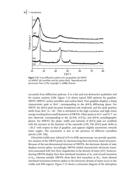
Figure 1.12 X-ray diffraction patterns for (a) graphite; (b) SWNT;<br />
(c) MWNT; (d) nanofiber <strong>and</strong> (e) carbon black. Reproduced with<br />
permission from [119]. Copyright Ó (2006) Elsevier.<br />
accurately from diffraction patterns. It is a fast <strong>and</strong> non-destructive qualitative tool<br />
for routine analysis [120]. Figure 1.12 shows typical XRD patterns for graphite,<br />
SWNT, MWNT, carbon nanofiber <strong>and</strong> carbon black. Pure graphite displays a sharp<br />
characteristic peak at 26.6 , corresponding to the (0 0 2) diffracting plane. For<br />
SWNT, the (0 0 2) peak becomes broadened <strong>and</strong> weakened, <strong>and</strong> the peak position<br />
shifts from 26.6 to 26 . This is attributed to the high curvature <strong>and</strong> high strain<br />
energy resulting from small diameters of SWNTs. Other peaks at 44.5 <strong>and</strong> 51.7 are<br />
also observed, corresponding to the {(1 0 0), (1 0 1)}, <strong>and</strong> (0 0 4) crystallographic<br />
planes. For MWNT, the shape, width <strong>and</strong> intensity of (0 0 2) peak are modified<br />
with the increase in the diameter of the nanotube [119]. The (0 0 2) peak shifts to<br />
26.2 with respect to that of graphite, <strong>and</strong> appears slightly asymmetric towards<br />
lower angles. The asymmetry is due to the presence of different crystalline<br />
species [120, 126].<br />
Ultraviolet-visible-near infrared (UV-vis-NIR) spectroscopy can provide quantitative<br />
analysis of the SWNT purity by characterizing their electronic b<strong>and</strong> structures.<br />
Because of the one-dimensional structure of SWNTs, the electronic density of state<br />
displays several spikes. Accordingly, SWNTs exhibit characteristic electronic transitions<br />
associated with Van Hove singularities in the density of states [127]. Semiconducting<br />
SWNTs display their first interb<strong>and</strong> transition at S11 <strong>and</strong> second transition<br />
at S22, whereas metallic SWNTs show their first transition at M11. Such allowed<br />
interb<strong>and</strong> transitions between spikes in the electronic density of states occur in the<br />
visible <strong>and</strong> NIR regions. Figure 1.13 shows a schematic diagram of the absorption