

TMS320C6713B Floating-Point Digital Signal Processor (Rev. A)
TMS320C6713B Floating-Point Digital Signal Processor (Rev. A)
TMS320C6713B Floating-Point Digital Signal Processor (Rev. A)

Create successful ePaper yourself
Turn your PDF publications into a flip-book with our unique Google optimized e-Paper software.
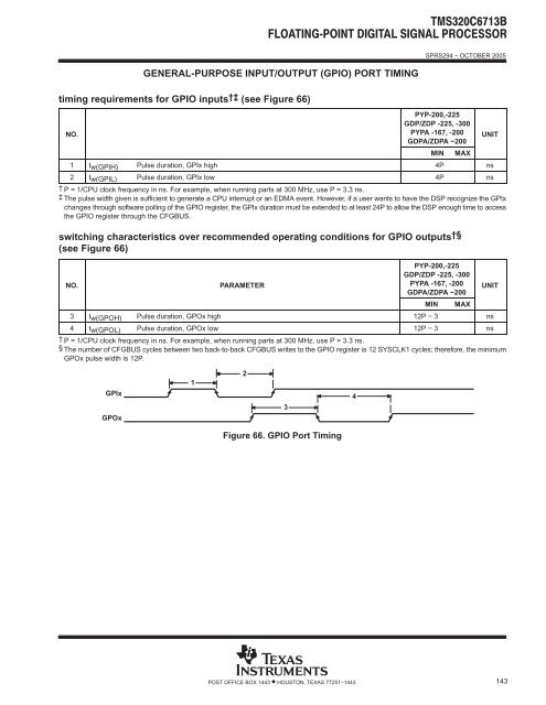
GENERAL-PURPOSE INPUT/OUTPUT (GPIO) PORT TIMING<br />
SPRS294 − OCTOBER 2005<br />
timing requirements for GPIO inputs †‡ (see Figure 66)<br />
NO.<br />
PYP-200,-225<br />
GDP/ZDP -225, -300<br />
PYPA -167, -200 UNIT<br />
GDPA/ZDPA −200<br />
MIN MAX<br />
1 tw(GPIH) Pulse duration, GPIx high 4P ns<br />
2 tw(GPIL) Pulse duration, GPIx low 4P ns<br />
† P = 1/CPU clock frequency in ns. For example, when running parts at 300 MHz, use P = 3.3 ns.<br />
‡ The pulse width given is sufficient to generate a CPU interrupt or an EDMA event. However, if a user wants to have the DSP recognize the GPIx<br />
changes through software polling of the GPIO register, the GPIx duration must be extended to at least 24P to allow the DSP enough time to access<br />
the GPIO register through the CFGBUS.<br />
switching characteristics over recommended operating conditions for GPIO outputs †§<br />
(see Figure 66)<br />
NO.<br />
PARAMETER<br />
PYP-200,-225<br />
GDP/ZDP -225, -300<br />
PYPA -167, -200 UNIT<br />
GDPA/ZDPA −200<br />
MIN MAX<br />
3 tw(GPOH) Pulse duration, GPOx high 12P − 3 ns<br />
4 tw(GPOL) Pulse duration, GPOx low 12P − 3 ns<br />
† P = 1/CPU clock frequency in ns. For example, when running parts at 300 MHz, use P = 3.3 ns.<br />
§ The number of CFGBUS cycles between two back-to-back CFGBUS writes to the GPIO register is 12 SYSCLK1 cycles; therefore, the minimum<br />
GPOx pulse width is 12P.<br />
GPIx<br />
GPOx<br />
1<br />
2<br />
3<br />
4<br />
Figure 66. GPIO Port Timing<br />
POST OFFICE BOX 1443 • HOUSTON, TEXAS 77251−1443<br />
143


