

TMS320C6713B Floating-Point Digital Signal Processor (Rev. A)
TMS320C6713B Floating-Point Digital Signal Processor (Rev. A)
TMS320C6713B Floating-Point Digital Signal Processor (Rev. A)

You also want an ePaper? Increase the reach of your titles
YUMPU automatically turns print PDFs into web optimized ePapers that Google loves.
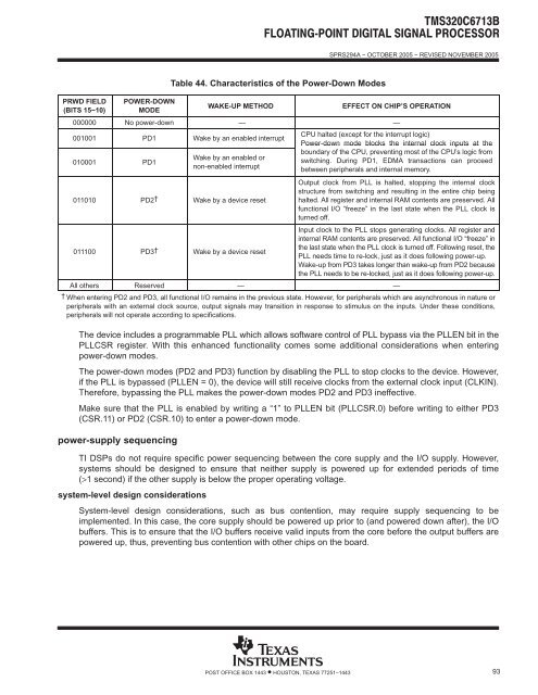
SPRS294A − OCTOBER 2005 − REVISED NOVEMBER 2005<br />
PRWD FIELD<br />
(BITS 15−10)<br />
POWER-DOWN<br />
MODE<br />
Table 44. Characteristics of the Power-Down Modes<br />
WAKE-UP METHOD<br />
EFFECT ON CHIP’S OPERATION<br />
000000 No power-down — —<br />
001001 PD1 Wake by an enabled interrupt<br />
CPU halted (except for the interrupt logic)<br />
Power-down mode blocks the internal clock inputs at the<br />
010001 PD1<br />
boundary of the CPU, preventing most of the CPU’s logic from<br />
Wake by an enabled or<br />
switching. During PD1, EDMA transactions can proceed<br />
non-enabled interrupt<br />
between peripherals and internal memory.<br />
011010 PD2† Wake by a device reset<br />
011100 PD3† Wake by a device reset<br />
Output clock from PLL is halted, stopping the internal clock<br />
structure from switching and resulting in the entire chip being<br />
halted. All register and internal RAM contents are preserved. All<br />
functional I/O “freeze” in the last state when the PLL clock is<br />
turned off.<br />
Input clock to the PLL stops generating clocks. All register and<br />
internal RAM contents are preserved. All functional I/O “freeze” in<br />
the last state when the PLL clock is turned off. Following reset, the<br />
PLL needs time to re-lock, just as it does following power-up.<br />
Wake-up from PD3 takes longer than wake-up from PD2 because<br />
the PLL needs to be re-locked, just as it does following power-up.<br />
All others Reserved — —<br />
† When entering PD2 and PD3, all functional I/O remains in the previous state. However, for peripherals which are asynchronous in nature or<br />
peripherals with an external clock source, output signals may transition in response to stimulus on the inputs. Under these conditions,<br />
peripherals will not operate according to specifications.<br />
The device includes a programmable PLL which allows software control of PLL bypass via the PLLEN bit in the<br />
PLLCSR register. With this enhanced functionality comes some additional considerations when entering<br />
power-down modes.<br />
The power-down modes (PD2 and PD3) function by disabling the PLL to stop clocks to the device. However,<br />
if the PLL is bypassed (PLLEN = 0), the device will still receive clocks from the external clock input (CLKIN).<br />
Therefore, bypassing the PLL makes the power-down modes PD2 and PD3 ineffective.<br />
Make sure that the PLL is enabled by writing a “1” to PLLEN bit (PLLCSR.0) before writing to either PD3<br />
(CSR.11) or PD2 (CSR.10) to enter a power-down mode.<br />
power-supply sequencing<br />
TI DSPs do not require specific power sequencing between the core supply and the I/O supply. However,<br />
systems should be designed to ensure that neither supply is powered up for extended periods of time<br />
(>1 second) if the other supply is below the proper operating voltage.<br />
system-level design considerations<br />
System-level design considerations, such as bus contention, may require supply sequencing to be<br />
implemented. In this case, the core supply should be powered up prior to (and powered down after), the I/O<br />
buffers. This is to ensure that the I/O buffers receive valid inputs from the core before the output buffers are<br />
powered up, thus, preventing bus contention with other chips on the board.<br />
POST OFFICE BOX 1443 • HOUSTON, TEXAS 77251−1443<br />
93


