

TMS320C6713B Floating-Point Digital Signal Processor (Rev. A)
TMS320C6713B Floating-Point Digital Signal Processor (Rev. A)
TMS320C6713B Floating-Point Digital Signal Processor (Rev. A)

Create successful ePaper yourself
Turn your PDF publications into a flip-book with our unique Google optimized e-Paper software.
SPRS294 − OCTOBER 2005<br />
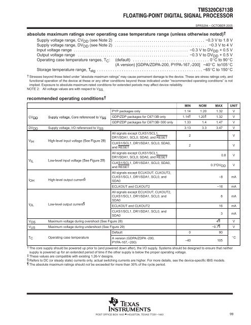
absolute maximum ratings over operating case temperature range (unless otherwise noted) †<br />
Supply voltage range, CV DD (see Note 2) . . . . . . . . . . . . . . . . . . . . . . . . . . . . . . . . . . . . . . . . . . . . −0.3 V to 1.8 V<br />
Supply voltage range, DV DD (see Note 2) . . . . . . . . . . . . . . . . . . . . . . . . . . . . . . . . . . . . . . . . . . . . . −0.3 V to 4 V<br />
Input voltage range . . . . . . . . . . . . . . . . . . . . . . . . . . . . . . . . . . . . . . . . . . . . . . . . . . . . . . . . −0.3 V to DV DD + 0.5 V<br />
Output voltage range . . . . . . . . . . . . . . . . . . . . . . . . . . . . . . . . . . . . . . . . . . . . . . . . . . . . . . −0.3 V to DV DD + 0.5 V<br />
Operating case temperature ranges, T C : (default) . . . . . . . . . . . . . . . . . . . . . . . . . . . . . . . . . . 0C to 90C<br />
(A version) [GDPA/ZDPA-200, PYPA-167,-200] −40C to105C<br />
Storage temperature range, T stg . . . . . . . . . . . . . . . . . . . . . . . . . . . . . . . . . . . . . . . . . . . . . . . −65C to 150C<br />
† Stresses beyond those listed under “absolute maximum ratings” may cause permanent damage to the device. These are stress ratings only, and<br />
functional operation of the device at these or any other conditions beyond those indicated under “recommended operating conditions” is not<br />
implied. Exposure to absolute-maximum-rated conditions for extended periods may affect device reliability.<br />
NOTE 2: All voltage values are with respect to VSS.<br />
recommended operating conditions †<br />
MIN NOM MAX UNIT<br />
PYP packages only 1.14 1.20 1.32 V<br />
CVDD<br />
Supply voltage, Core referenced to VSS GDP/ZDP packages for C6713B only 1.14‡ 1.20‡ 1.32 V<br />
GDP/ZDP packages for C6713B−300 only 1.33 1.4 1.47 V<br />
DVDD Supply voltage, I/O referenced to VSS 3.13 3.3 3.47 V<br />
VIH High-level input voltage (See Figure 28)<br />
VIL Low-level input voltage (See Figure 29)<br />
IOH<br />
IOL<br />
High-level output current§<br />
Low-level output current§<br />
All signals except CLKS1/SCL1,<br />
DR1/SDA1, SCL0, SDA0, and RESET<br />
CLKS1/SCL1, DR1/SDA1, SCL0, SDA0,<br />
and RESET<br />
All signals except CLKS1/SCL1,<br />
DR1/SDA1, SCL0, SDA0, and RESET<br />
CLKS1/SCL1, DR1/SDA1, SCL0, SDA0,<br />
and RESET<br />
2 V<br />
2 V<br />
0.3*DVDD<br />
0.8 V<br />
All signals except ECLKOUT, CLKOUT2,<br />
CLKS1/SCL1, DR1/SDA1, SCL0, and<br />
SDA0<br />
−8 mA<br />
ECLKOUT and CLKOUT2 −16 mA<br />
All signals except ECLKOUT, CLKOUT2,<br />
CLKS1/SCL1, DR1/SDA1, SCL0, and<br />
8 mA<br />
SDA0<br />
ECLKOUT and CLKOUT2 16 mA<br />
CLKS1/SCL1, DR1/SDA1, SCL0, and<br />
3 mA<br />
SDA0<br />
VOS Maximum voltage during overshoot (See Figure 28) 4 V<br />
VUS Maximum voltage during undershoot (See Figure 29) −0.7 V<br />
TC Operating case temperature A version (GDPA/ZDPA -200,<br />
PYPA-167,−200)<br />
Default 0 90<br />
–40 105<br />
† The core supply should be powered up prior to (and powered down after), the I/O supply. Systems should be designed to ensure that neither<br />
supply is powered up for an extended period of time if the other supply is below the proper operating voltage.<br />
‡ These values are compatible with existing 1.26-V designs.<br />
§ Refers to DC (or steady state) currents only, actual switching currents are higher. For more details, see the device-specific IBIS models.<br />
The absolute maximum ratings should not be exceeded for more than 30% of the cycle period.<br />
V<br />
C<br />
POST OFFICE BOX 1443 • HOUSTON, TEXAS 77251−1443<br />
99


