

TMS320C6713B Floating-Point Digital Signal Processor (Rev. A)
TMS320C6713B Floating-Point Digital Signal Processor (Rev. A)
TMS320C6713B Floating-Point Digital Signal Processor (Rev. A)

Create successful ePaper yourself
Turn your PDF publications into a flip-book with our unique Google optimized e-Paper software.
SPRS294A − OCTOBER 2005 − REVISED NOVEMBER 2005<br />
PLL and PLL controller (continued)<br />
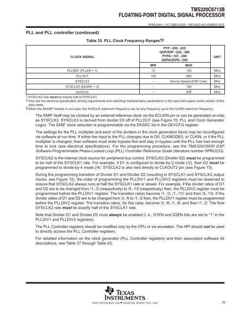
Table 35. PLL Clock Frequency Ranges †‡<br />
CLOCK SIGNAL<br />
PYP −200, -225<br />
GDP/ZDP −225, -300<br />
PYPA −167, -200<br />
UNIT<br />
GDPA/ZDPA −200<br />
MIN<br />
MAX<br />
PLLREF (PLLEN = 1) 12 100 MHz<br />
PLLOUT 140 600 MHz<br />
SYSCLK1 − Device Speed (DSP Core) MHz<br />
SYSCLK3 (EKSRC = 0) − 100 MHz<br />
AUXCLK − 50§ MHz<br />
† SYSCLK2 rate must be exactly half of SYSCLK1.<br />
‡ Also see the electrical specification (timing requirements and switching characteristics parameters) in the input and output clocks section of this<br />
data sheet.<br />
§ When the McASP module is not used, the AUXCLK maximum frequency can be any frequency up to the CLKIN maximum frequency.<br />
The EMIF itself may be clocked by an external reference clock via the ECLKIN pin or can be generated on-chip<br />
as SYSCLK3. SYSCLK3 is derived from divider D3 off of PLLOUT (see Figure 15, PLL and Clock Generator<br />
Logic). The EMIF clock selection is programmable via the EKSRC bit in the DEVCFG register.<br />
The settings for the PLL multiplier and each of the dividers in the clock generation block may be reconfigured<br />
via software at run time. If either the input to the PLL changes due to D0, CLKMODE0, or CLKIN, or if the PLL<br />
multiplier is changed, then software must enter bypass first and stay in bypass until the PLL has had enough<br />
time to lock (see electrical specifications). For the programming procedure, see the TMS320C6000 DSP<br />
Software-Programmable Phase-Locked Loop (PLL) Controller Reference Guide (literature number SPRU233).<br />
SYSCLK2 is the internal clock source for peripheral bus control. SYSCLK2 (Divider D2) must be programmed<br />
to be half of the SYSCLK1 rate. For example, if D1 is configured to divide-by-2 mode (/2), then D2 must be<br />
programmed to divide-by-4 mode (/4). SYSCLK2 is also tied directly to CLKOUT2 pin (see Figure 15).<br />
During the programming transition of Divider D1 and Divider D2 (resulting in SYSCLK1 and SYSCLK2 output<br />
clocks, see Figure 15), the order of programming the PLLDIV1 and PLLDIV2 registers must be observed to<br />
ensure that SYSCLK2 always runs at half the SYSCLK1 rate or slower. For example, if the divider ratios of D1<br />
and D2 are to be changed from /1, /2 (respectively) to /5, /10 (respectively) then, the PLLDIV2 register must be<br />
programmed before the PLLDIV1 register. The transition ratios become /1, /2; /1, /10; and then /5, /10. If the<br />
divider ratios of D1 and D2 are to be changed from /3, /6 to /1, /2 then, the PLLDIV1 register must be programmed<br />
before the PLLDIV2 register. The transition ratios, for this case, become /3, /6; /1, /6; and then /1, /2. The final<br />
SYSCLK2 rate must be exactly half of the SYSCLK1 rate.<br />
Note that Divider D1 and Divider D2 must always be enabled (i. e., D1EN and D2EN bits are set to “1” in the<br />
PLLDIV1 and PLLDIV2 registers).<br />
The PLL Controller registers should be modified only by the CPU or via emulation. The HPI should not be used<br />
to directly access the PLL Controller registers.<br />
For detailed information on the clock generator (PLL Controller registers) and their associated software bit<br />
descriptions, see Table 37 through Table 43.<br />
POST OFFICE BOX 1443 • HOUSTON, TEXAS 77251−1443<br />
79


